1 mode register definition, 2 extended mode register definition – Freescale Semiconductor MCF5480 User Manual
Page 460
MCF548x Reference Manual, Rev. 3
18-12
Freescale Semiconductor
18.5.1.5.1
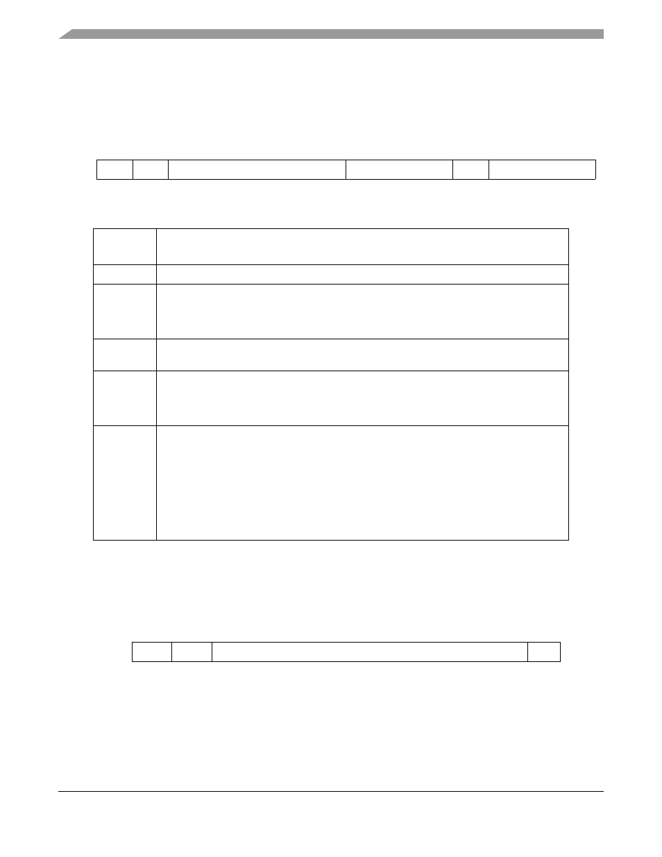
Mode Register Definition
shows the mode register definition. Note that this is the SDRAM’s mode register not the
SDRAMC’s mode/extended mode register (SDMR) defined in
Section 18.7.3, “SDRAM Mode/Extended
18.5.1.5.2
Extended Mode Register Definition
shows the extended mode register used by DDR SDRAMs. Note that this is the SDRAM’s
extended mode register, not the SDRAMC’s mode/extended mode register (SDMR) defined in
Section 18.7.3, “SDRAM Mode/Extended Mode Register (SDMR)
.”
BA1
BA0
A11
A10
A9
A8
A7
A6
A5
A4
A3
A2
A1
A0
Field
0
0
OP_MODE
CASL
BT
BLEN
Figure 18-6. Mode Register
Table 18-4. Mode Register Field Descriptions
Address
Line
Description
BA[1:0]
Bank Address. These must both be zero to select the mode register.
A11–A7
Operating Mode.
00000 Normal Operation
00010 Reset DLL
Other values should not be used.
A6–A4
CAS latency. Delay in clocks from issuing a READ to valid data out. Check the SDRAM
manufacturer’s spec as the CASL settings supported can vary from memory to memory.
A3
Burst Type.
0 Sequential
1 Interleaved. This setting should not be used since the SDRAMC does not support interleaved
bursts.
A2–A0
Burst length. Determines the number of locations that are accessed for a single READ or
WRITE.
000 One. This is only a valid setting for SDR.
001 Two
010 Four
011 Eight (This value should be used for the MCF548x SDRAMC)
100–110 Reserved
111 Full page. This setting should not be used since full page bursting is not supported by the
SDRAMC.
BA1
BA0
A11
A10
A9
A8
A7
A6
A5
A4
A3
A2
A1
A0
Field
0
1
OPTION
DLL
Figure 18-7. Extended Mode Register