Chapter 10 internal clocks and bus architecture, 1 introduction, 1 block diagram – Freescale Semiconductor MCF5480 User Manual
Page 323: Chapter 10, Internal clocks and bus architecture, Introduction -1, Block diagram -1, Chapter 10, “internal clocks and bus architecture
MCF548x Reference Manual, Rev. 3
Freescale Semiconductor
10-1
Chapter 10
Internal Clocks and Bus Architecture
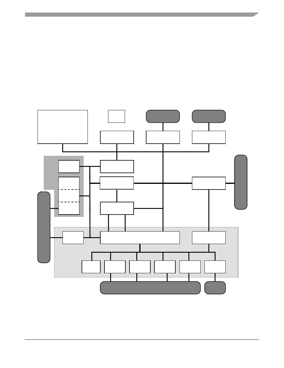
10.1
Introduction
This chapter describes the clocking and internal buses of the MCF548x and discusses the main functional
blocks controlling the XL bus and the XL bus arbiter.
10.1.1
Block Diagram
shows a top-level block diagram of the MCF548x products.
*Available in MCF5485, MCF5484, MCF5483, and MCF5482 devices.
**Available in MCF5485, MCF5484, MCF5481, and MCF5480 devices.
***Available in MCF5485, MCF5483, and MCF5481 devices.
Figure 10-1. MCF548x Internal Bus
Architecture
PLL
DDR SDRAM
Memory
Controller
PCI I/O Interfa
ce and Ports
CommBus
USB 2.0
PHY*
Perpheral Communications I/O Interface & Ports
FEC1**
PSC x 4
I
2
C
FEC0
USB 2.0
DEVICE*
Interface
FlexBus
Controller
FlexBus
Interface
PCI Interface
& FIFOs
Master/Slave
Interface
ColdFire V4e Core
FPU, MMU
EMAC
32K D-cache
32K I-cache
FlexCAN
x 2
Slave
Bus
DSPI
Perpher
a
l I/O Interface &
Ports
Co
mmuni
ca
tions
I/O S
ubs
ys
te
m
Interrupt
Controller
XL Bus
Arbiter
Sy
st
em
In
te
gr
at
io
n U
nit
DM
A
Re
ad
DMA
Wr
ite
Multichannel DMA
Master Bus Interface and FIFOs
Slice
Timers x 2
GP
Timers x 4
Watchdog
Timer
PCI 2.2
Controller
Cryptography
32K System
SRAM
Cry
pto
R/W
XL Bus
Read/Write
XL Bus
Accelerator***