Figure 18-18, Along with the base settings for the sdcr – Freescale Semiconductor MCF5480 User Manual
Page 476
MCF548x Reference Manual, Rev. 3
18-28
Freescale Semiconductor
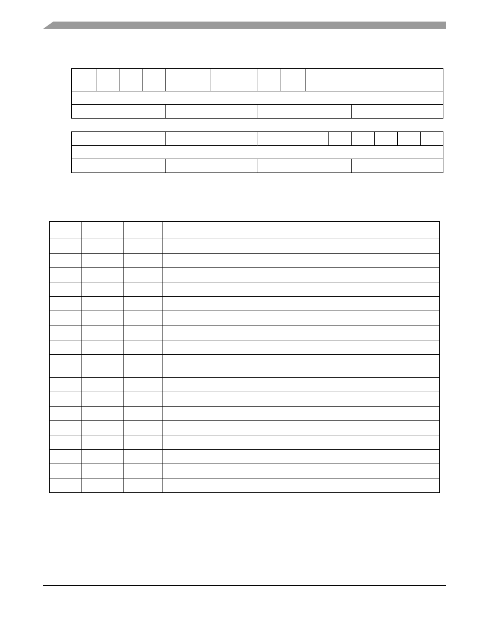
This configuration results in a value of SDCR = 0xE10D_0002, as described in
Table 18-19
.
31
30
29
28
27
26
25
24
23
22
21
20
19
18
17
16
Field MODE
_EN
CKE
DDR
REF
—
MUX
AP
DRIVE
RCNT
Setting
1110_0001_0000_1101
(hex)
E
1
0
D
15
14
13
12
11
10
9
8
7
6
5
4
3
2
1
0
Field
—
DQS_OE
—
BUFF
—
IREF IPALL
—
Setting
0000_0000_0000_0010
(hex)
0
0
0
2
Figure 18-18. SDRAM Control Register Settings + MODE_EN and IPALL
Table 18-19. SDCR + MODE_EN and IPALL Field Descriptions
Bits
Name
Setting
Description
31
MODE_EN
1
Mode register is writable.
30
CKE
1
SDCKE is asserted
29
DDR
1
DDR mode is enabled
28
REF
0
Automatic refresh is disabled
27–26
—
00
Reserved. Should be cleared.
25–24
MUX
01
01 is the MUX setting for a 13 x 9 x 4 memory. See
.
23
AP
0
0 sets the auto precharge control bit to A10.
22
DRIVE
0
Data and DQS lines are only driven for a write cycle.
21–16
RCNT
001101
RCNT = (t
REFI
/ (SDCLK x 64)) - 1 = (7800ns/(8.3ns x 64)) - 1 = 13.62, round down to
13 (0xD)
15–12
—
0000
Reserved. Should be cleared.
11–8
DQS_OE
0000
0x0 disables drive for all SDDQS pins for now.
7–5
—
000
Reserved. Should be cleared.
4
BUFF
0
0 indicates that a buffered memory module is not being used.
3
—
0
Reserved. Should be cleared.
2
IREF
0
Do not initiate a REF command.
1
IPALL
1
Initiate a PALL command.
0
—
0
Reserved. Should be cleared.