3 memory map/register definition, 1 memory map, 2 register descriptions – Freescale Semiconductor MCF5480 User Manual
Page 368: Memory map/register definition -2, Memory map -2, Register descriptions -2
MCF548x Reference Manual, Rev. 3
14-2
Freescale Semiconductor
NOTE
The GPIO functionality of the external interrupt pins is controlled by the
EPORT module. However, some external interrupt signals are muxed with
other functions. In this case, the pin’s IRQ functionality must be enabled in
the GPIO module’s pin assignment register in order to use the pin’s GPIO
function via the EPORT registers. For more information, refer to
14.3
Memory Map/Register Definition
This subsection describes the memory map and register structure.
14.3.1
Memory Map
Refer to
for a description of the EPORT memory map. The EPORT has an MBAR offset for
base address of 0xF00.
14.3.2
Register Descriptions
The EPORT programming model consists of these registers:
•
The EPORT pin assignment register (EPPAR) controls the function of each pin individually.
•
The EPORT data direction register (EPDDR) controls the direction of each pin individually.
•
The EPORT interrupt enable register (EPIER) enables interrupt requests for each pin individually.
•
The EPORT data register (EPDR) holds the data to be driven to the pins.
•
The EPORT pin data register (EPPDR) reflects the current state of the pins.
•
The EPORT flag register (EPFR) individually latches EPORT edge events.
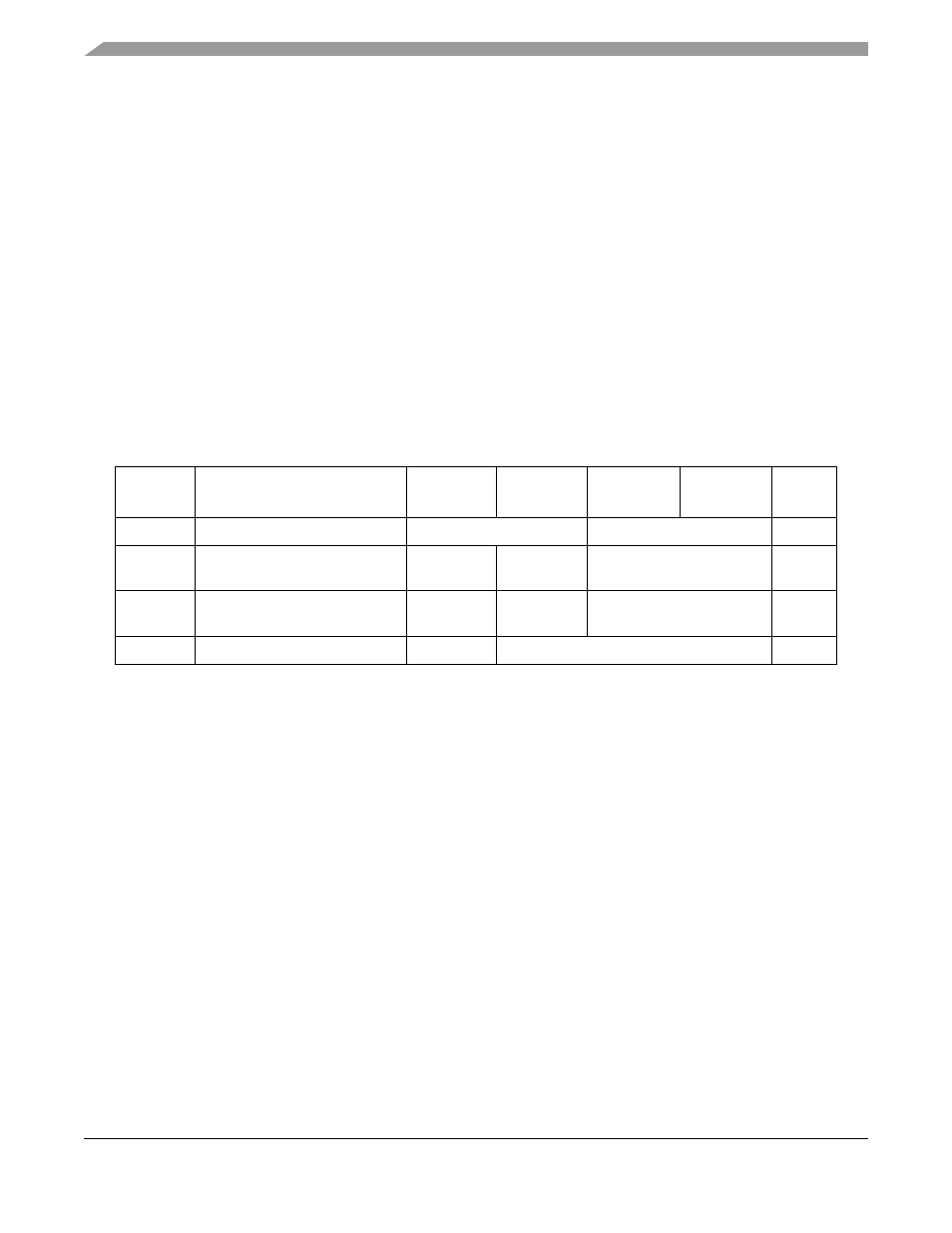
Table 14-1. Edge Port Module Memory Map
MBAR
Offset
Name
Byte0
Byte1
Byte2
Byte3
Access
1
1
S = CPU supervisor mode access only. S/U = CPU supervisor or user mode access. User mode accesses to
supervisor only addresses have no effect and result in a cycle termination transfer error.
0xF00
EPORT pin assignment register
EPPAR
—
2
S
0xF04
EPORT data direction register
EPORT interrupt enable register
EPDDR
EPIER
—
2
2
Writing to reserved address locations has no effect, and reading returns 0s.
S/U
0xF08
EPORT data register
EPORT pin data register
EPDR
EPPDR
—
2
0xF0C
EPORT flag register
EPFR
—
2