7 functional description, Functional description -18 – Freescale Semiconductor MCF5480 User Manual
Page 836
MCF548x Reference Manual, Rev. 3
27-18
Freescale Semiconductor
27.7
Functional Description
The DMA serial peripheral interface (DSPI) block provides a synchronous serial bus for communication
between an MCU and an external peripheral device. The DSPI supports up to eight queued SPI transfers
at once (four transmit and four receive) in the DSPI resident FIFOs, thereby eliminating CPU intervention
between transfers.
The DCTARn registers hold clock and transfer attributes. The SPI configuration can select which CTAR
to use on a frame-by-frame basis by setting a field in the SPI command. See
and Transfer Attributes Registers 0–7 (DCTARn)
” for information on the fields of the DCTAR registers.
The 16-bit shift register in the master and the 16-bit shift register in the slave are linked by the DSPISOUT
and DSPISIN signals to form a distributed 32-bit register. When a data transfer operation is performed,
data is serially shifted a predetermined number of bit positions. Because the registers are linked, data is
exchanged between the master and the slave; the data that was in the master’s shift register is now in the
shift register of the slave, and vice versa. At the end of a transfer, the DSR[TCF] bit is set to indicate a
completed transfer.
illustrates how master and slave data is exchanged.
31
30
29
28
27
26
25
24
23
22
21
20
19
18
17
16
R
0
0
0
0
0
0
0
0
0
0
0
0
0
0
0
0
W
Reset
0
0
0
0
0
0
0
0
0
0
0
0
0
0
0
0
15
14
13
12
11
10
9
8
7
6
5
4
3
2
1
0
R
RXDATA
W
Reset
0
0
0
0
0
0
0
0
0
0
0
0
0
0
0
0
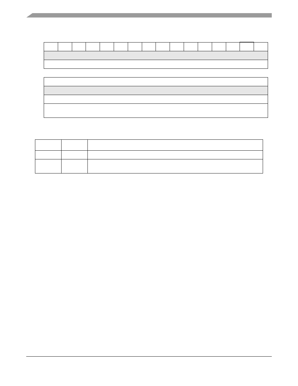
Reg
Addr
MBAR + 0x8A7C–8A88
Figure 27-10. DSPI Rx FIFO Debug Register (DRFDR_x)
Table 27-13. DRFDR_x Field Descriptions
Bits
Name
Description
31–16
—
Reserved, should be cleared.
15–0
RXDATA
Received data. The RXDATA field contains the SPI data from the Rx FIFO entry pointed to
by the receive next data pointer.