Freescale Semiconductor MCF5480 User Manual
Page 470
MCF548x Reference Manual, Rev. 3
18-22
Freescale Semiconductor
The minimum values of certain fields can be different for SDR and DDR SDRAM, even if the data sheet
timing is the same, because:
•
In SDR mode, the memory controller counts the delay in SDCLK
•
In DDR mode, the memory controller counts the delay in SDCLK
× 2
SDCLK—memory controller clock—is the speed of the SDRAM interface and is equal to the internal bus
clock.
SDCLK
× 2—double frequency of SDCLK—DDR uses both edges of the bus-frequency clock (SDCLK)
to read/write data
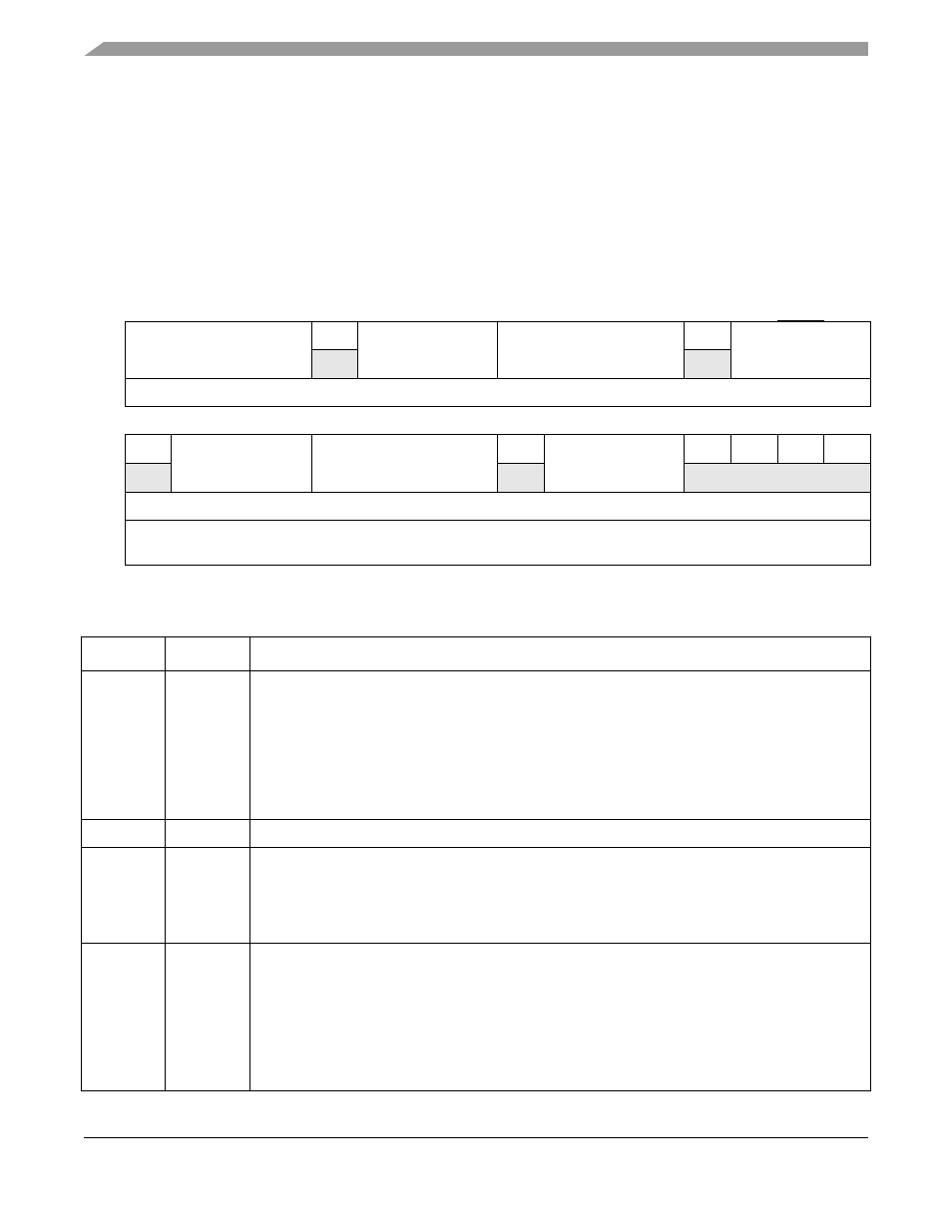
31
30
29
28
27
26
25
24
23
22
21
20
19
18
17
16
R
SRD2RW
0
SWT2RD
RDLAT
0
ACT2RW
W
Reset
Uninitialized
15
14
13
12
11
10
9
8
7
6
5
4
3
2
1
0
R
0
PRE2ACT
REF2ACT
0
WTLAT
0
0
0
0
W
Reset
Uninitialized
Reg
Addr
MBAR + 0x0108
Figure 18-12. SDRAM Configuration Register 1 (SDCFG1)
Table 18-12. SDCFG1 Field Descriptions
Bits
Name Description
31–28
SRD2RW
Single Read to Read/Write/Precharge delay. Limiting case is usually Write to Precharge.
DDR mode:
SRD2RW = CASL + (BL/2) + 1
For DDR, suggested value = 0x7
SDR mode:
SRD2RW = CASL + BL + 1
If CASL=2, suggested value = 0xB
If CASL=3, suggested value = 0xC
27
—
Reserved. should be cleared
26–24
SWT2RD
Single Write to Read/Write/Precharge delay. Limiting case is Write to Precharge.
DDR mode:
SWT2RD = t
WR
/SDCLK + 1, suggested value = 0x3
SDR mode:
SWT2RD = t
WR
, suggested value = 0x2
23–20
RDLAT
Read CAS Latency. Read latency. Read command to read data available delay counter.
DDR mode:
If CASL = 2, write 0x6
If CASL = 2.5, write 0x7
SDR mode:
If CASL = 2, write 0x2
If CASL = 3, write 0x3
Note: CASL=2.5 is not supported for SDR.