3 register descriptions, 1 mode register 1(pscmr1n), Register descriptions -5 – Freescale Semiconductor MCF5480 User Manual
Page 767: Mode register 1(pscmr1n) -5, 1 mode register 1(pscmr1 n )
Memory Map/Register Definition
MCF548x Reference Manual, Rev. 3
Freescale Semiconductor
26-5
26.3.3
Register Descriptions
This section gives detailed descriptions of the user accessible registers and bits within the module. In cases
where the operation mode affects the functionality of the control register, the operation in each mode is
described.
NOTE
Bit functions can vary in different operating modes. The field descriptions
are labelled to indicate which modes use a particular field.
26.3.3.1
Mode Register 1(PSCMR1n)
PSCMR1 controls some of the module configurations. It can be read or written at any time. It is accessed
when the mode register pointer points to PSCMR1. The pointer is set to mode register 1 by reset or by a
set pointer command using the MISC[2:0] bits in the command register (PSCCR). The pointer points to
the next mode register, PSCMR2, after reading or writing PSCMR1.
0x868E
0x878E
0x888E
0x898E
PSC TxFIFO Alarm Register
—
PSCTFAR
R/W
0x8692
0x8792
0x8892
0x8992
PSC TxFIFO Read Pointer
—
PSCTFRP
R/W
0x8696
0x8796
0x8896
0x8996
PSC TxFIFO Write Pointer
—
PSCTFWP
R/W
0x869A
0x879A
0x889A
0x899A
PSC TxFIFO Last Read Frame
Pointer
—
PSCTLRFP
R/W
0x869E
0x879E
0x889E
0x899E
PSC TxFIFO Last Write Frame
Pointer
—
PSCTLWFP
R/W
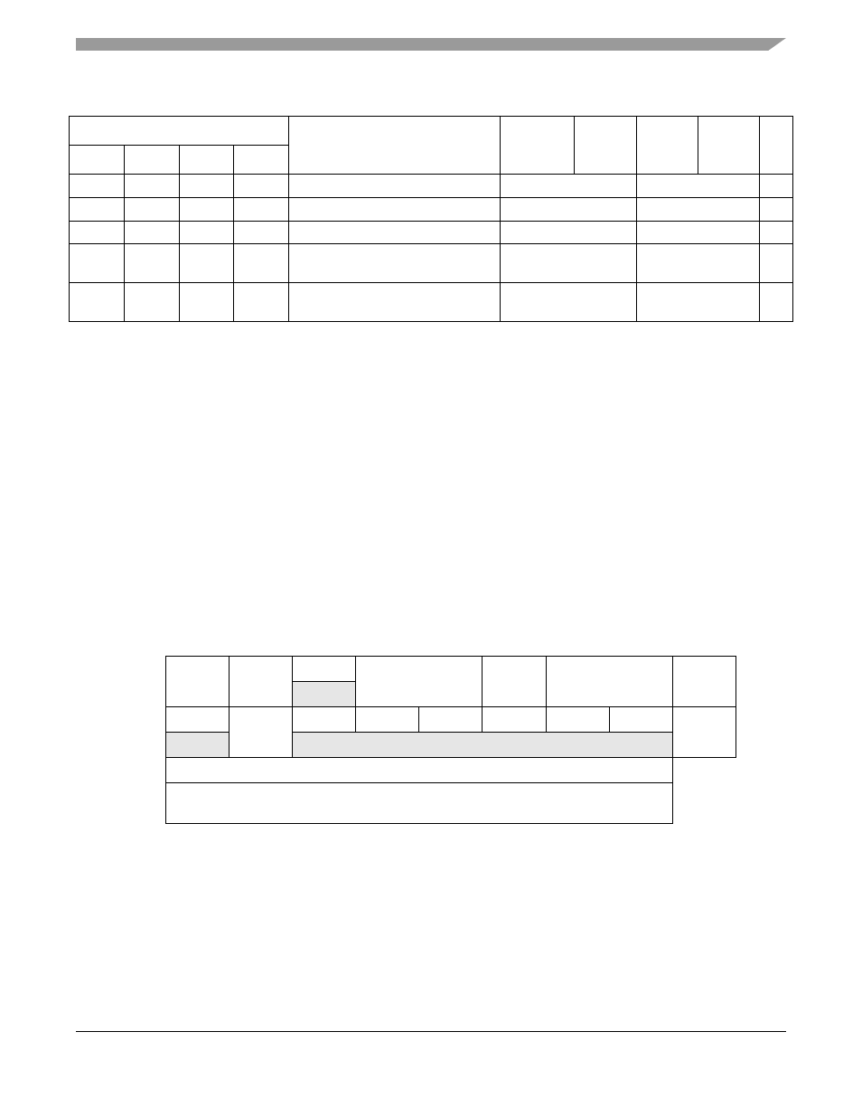
7
6
5
4
3
2
1
0
Mode
R
RXRTS
RXIRQ /
FU
ERR
PM
PT
BC
UART
W
R
0
RXIRQ
0
0
0
0
0
0
All other
modes
W
Reset
0
0
1
0
0
0
0
0
Reg
Addr
MBAR + 0x8600 (PSC0); 0x8700 (PSC1); 0x8800 (PSC2); 0x8900 (PSC3)
Figure 26-2. PSC Mode Register 1 (PSCMR1n)
Table 26-2. PSC Memory Map (Continued)
MBAR Offset
Name
Byte0
Byte1
Byte2
Byte3
Acce
ss
PSC0
PSC1
PSC2
PSC3