1 transmitter, 2 receiver, 3 low power mode – Freescale Semiconductor MCF5480 User Manual
Page 802: Transmitter -40, Receiver -40, Low power mode -40
MCF548x Reference Manual, Rev. 3
26-40
Freescale Semiconductor
26.4.5.1
Transmitter
The transmitter starts to transmit the first bit at the one clock after the rising edge of the frame sync. The
first slot, slot #0, is 16 bits wide while the other slot, from slot #1 to slot #12, is 20 bits wide. Because the
transmit order is the MSB first, the SHDIR bit in the PSCSICR should be a value 0. The transmitter keeps
the output low until the receiver detects the ‘CODEC ready’ condition, which is indicated by a high in the
first bit of a new frame. Since receive data is sampled on the falling edge of the bit clock, the frame has
already started when a ‘CODEC ready’ condition is detected by the receiver. For this reason, when the
‘CODEC ready’ condition is detected, a transmission starts at the next frame (one clock after the next
frame sync). The transmitter stops transmission from the beginning of the frame in which the first bit of
the receiver frame was detected to be low, i.e. CODEC is not ready. During transmission, the transmitter
fills each of the 13 time slots of the AC97 frame with samples from the TxFIFO.
26.4.5.2
Receiver
The receiver starts to receive slot #0 data one bit clock after the rising edge of a frame sync. Until the
receiver detects a ‘CODEC ready’ condition, no data is put into the RxFIFO for that frame. When a
‘CODEC ready’ is detected, the receiver starts loading the RxFIFO with the received time slot samples
and continues to do so until a 0 is received in the first bit of a new frame.
26.4.5.3
Low Power Mode
PSC monitors the first three timeslots of each transmitter frame in order to detect the power down
condition for the AC97 digital interface. Detection of the power down condition is done as follows:
1. The first three bits of slot #0 must be 1 indicating that this transmitter frame is valid, and that slots
#1 and #2 are valid.
2. Slot #1 contains the address of the power down register (26 hex)
3. Slot #2 contains a 1 in the fourth bit (bit 12/PR4 in power down register)
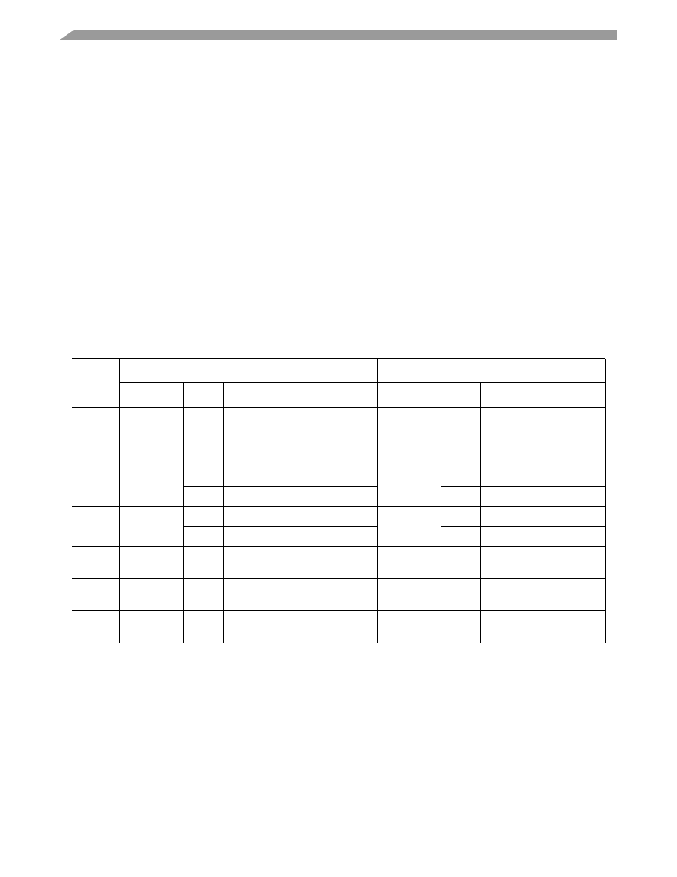
Table 26-37. Slot Functions in AC97
Slot
Number
Output (PSCnTXD)
Input (PSCnRXD)
Slot Name
Bit
Description
Slot Name
Bit
Description
Slot #0
Tag
15
Frame valid
Tag
15
CODEC ready
14
Control register address valid
14
Slot #1 data valid
13
Control register data valid
13
Slot #2 data valid
12
Left playback PCM data valid
12
Slot #3 data valid
11
Right playback PCM data valid
11
Slot #4 data valid
Slot #1
Control
address
19
Read/Write=1/0
Status
address
19
0
18:12
Control register number
18:12
Control register number
Slot #2
Control data
19:4
Write data.
0 in read
Status data
19:4
Control register read data
Slot #3
Left PCM
playback
19:0
PCM audio data left
Left PCM
record
19:0
PCM record data left
Slot #4
Right PCM
playback
19:0
PCM audio data right
Right PCM
record
19:0
PCM record data right