2 features, 3 overview, 2 memory map/register definition – Freescale Semiconductor MCF5480 User Manual
Page 410: Features -2, Overview -2, Memory map/register definition -2, Table 16-1/16-2
MCF548x Reference Manual, Rev. 3
16-2
Freescale Semiconductor
The system SRAM contents always reside at MBAR + 0x0001 0000; therefore, it can be relocated by
changing the MBAR contents.
16.1.2
Features
The 32-Kbyte system SRAM is intended primarily as a fast scratch memory and data buffer for DMA and
SEC processing, and as memory accessed through the shared bus by all system masters. The module
features are the following:
•
Four 8-Kbyte banks, each organized as 2048
× 32-bits
•
Dedicated 32-bit data bus per bank
•
Optionally interleaved along long-word boundaries under software control
•
Single cycle access when accessed by the DMA
•
Byte, word, and longword addressing capabilities
•
Independent arbitration mechanism per bank
16.1.3
Overview
This module provides a general-purpose memory block that can be accessed by the masters in the system
(ColdFire core, SEC, DMA, and PCI) via the shared internal system bus. The SRAM is also accessed
directly (without going through the system bus) by the SEC and DMA. This allows a mechanism for the
sharing of parameter data among the various masters as well as a dedicated fast scratch memory and data
buffer for DMA and SEC processing tasks.
In order to maximize concurrent utilization, the system SRAM is organized as four banks. Each master is
allocated a maximum transfer count and must give up access to the bank when its transfer count has been
depleted. In this fashion, each master is given the opportunity to access each bank to prevent starvation of
any given master. The transfer counts are configurable under software control for each master and each
bank, so it can be optimized to maximize the SRAM utilization for specific tasks. Optionally, a master can
be set to “own” a bank, whereby all other masters can access the bank only when the “own” master is not
making accesses to the bank.
16.2
Memory Map/Register Definition
shows the memory map of the system SRAM module. For more information about a particular
register, refer to the description of the register in the following sections.
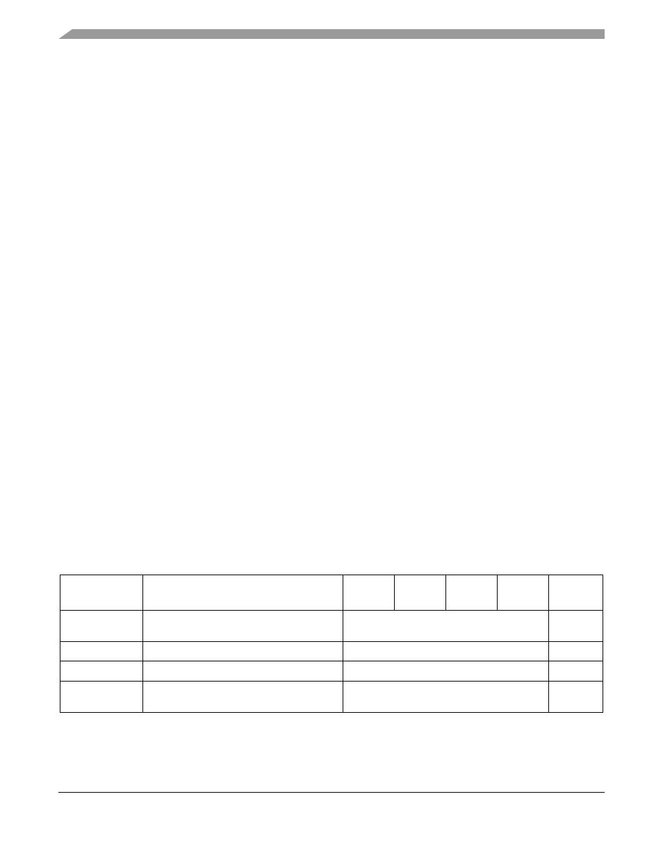
Table 16-1. System SRAM Memory Map
Address
(MBAR + )
Name
Byte 0
Byte 1
Byte 2
Byte 3
Access
0x1_0000–
0x1_7FFC
SRAM Contents
R/W
0x1_FFC0
System SRAM Configuration Register
SSCR
R/W
0x1_FFC4
Transfer Count Configuration Register
TCCR
R/W
0x1_FFC8
Transfer Count Configuration Register - DMA
Read Channel
TCCRDR
R/W