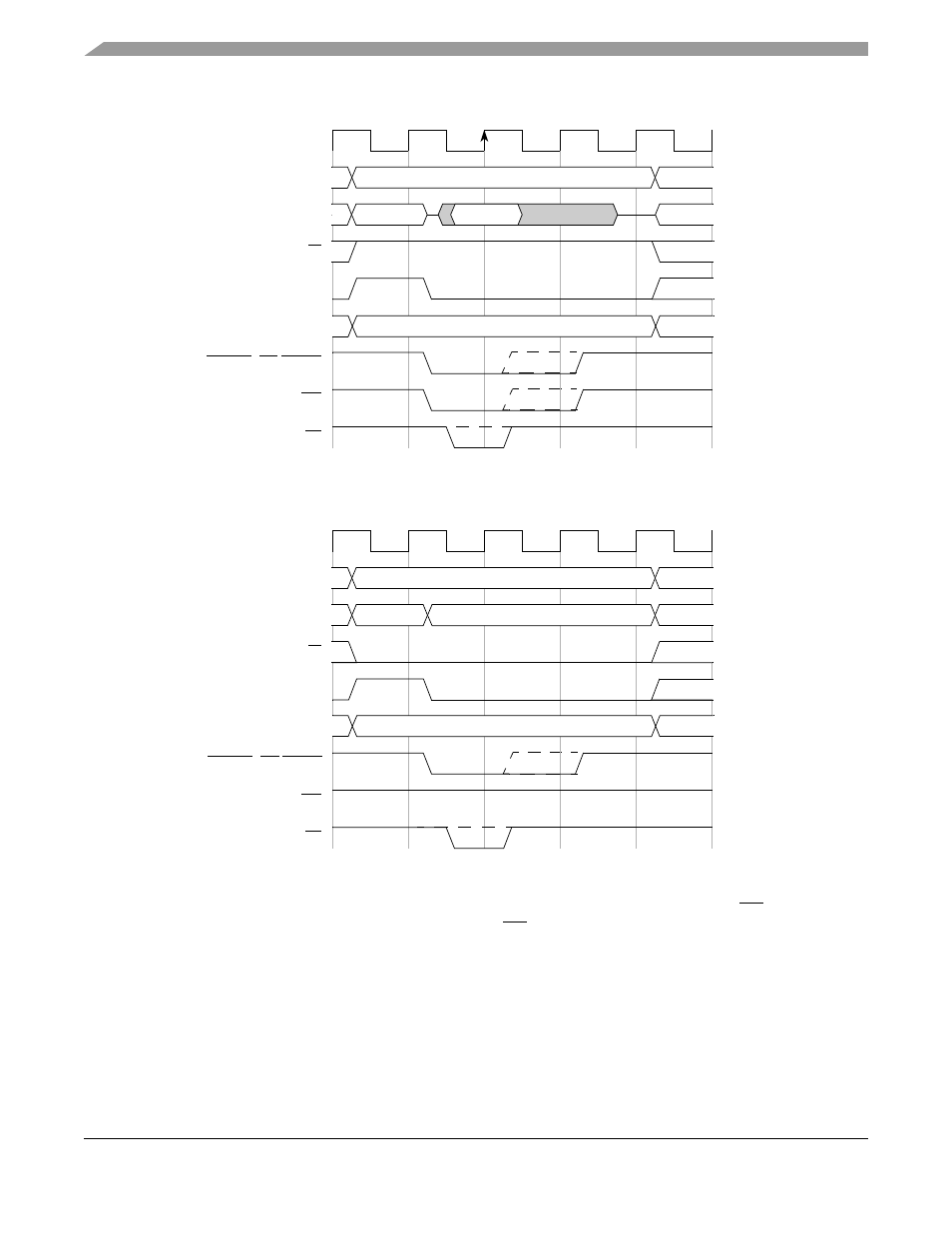
Figure 17-18, Figure 17-19, Show the basic read and writ – Freescale Semiconductor MCF5480 User Manual
Page 438
MCF548x Reference Manual, Rev. 3
17-22
Freescale Semiconductor
Figure 17-18. Basic Read Bus Cycle (No Wait States)
Figure 17-19. Basic Write Bus Cycle (No Wait States)
If wait states are used, then the S1 state will repeat continuously until either the internal TA is asserted by
the chip select auto-acknowledge unit or the external TA is recognized as asserted.
show a read and write cycle with one wait state.
CLK
AD[X:0]
AD[31:Y]
R/W
ALE
TA
OE
S0
S1
S2
S3
FBCSn, BE/BWEn
ADDR[X:0]
A[31:Y]
DATA
TSIZ[1:0]
TSIZ[1:0]
CLK
AD[X:0]
AD[31:Y]
R/W
ALE
TA
OE
S0
S1
S2
S3
FBCSn, BE/BWEn
ADDR[X:0]
A[31:Y]
DATA
TSIZ[1:0]
TSIZ[1:0]