1 module base address register (mbar), Module base address register (mbar) -2, Section 9.3.1, “module base address – Freescale Semiconductor MCF5480 User Manual
Page 318: Register (mbar)
MCF548x Reference Manual, Rev. 3
9-2
Freescale Semiconductor
9.3.1
Module Base Address Register (MBAR)
The supervisor-level MBAR,
, specifies the base address and allowable access types for all
internal peripherals. It is written with a MOVEC instruction using the CPU address 0xC0F (refer to the
ColdFire Family Programmer’s Reference Manual). MBAR can be read or written through the debug
modules as a read/write register, as described in
Only the debug module can
read MBAR.
The MBAR is initialized to 0x8000_0000 at reset; however, it can be relocated to a new base address. To
access internal peripherals, write MBAR with the appropriate base address (BA) after system reset.
All internal peripheral registers occupy a single relocatable memory block along 256-KByte boundaries.
MBAR[BA] is compared to the upper 14 bits of the full 32-bit internal address to determine if an internal
peripheral is being accessed. Any accesses in this range, whether to a valid peripheral address or not, will
be made internally rather than using the external bus.
NOTE
The MBAR region must be mapped to non-cacheable space.
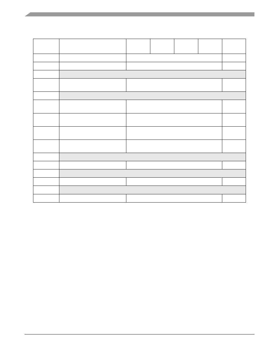
Table 9-1. SIU Register Map
Address
(MBAR +)
Name
Byte0
Byte1
Byte2
Byte3
Access
CPU+0xC0F
Module Base Address Register
MBAR
R/W
0x04
SDRAM Drive Strength Register
1
1
The SDRAM Drive Strength and Chip Select Configuration registers are discussed in
They are shown in this memory map for reference purposes.
SDRAMDS
1
R/W
0x08–0x0C
Reserved
0x10
System Breakpoint Control Regis-
ter
SBCR
R/W
0x1–0x1C
Reserved
0x20
SDRAM Chip Select 0
Configuration Register
1
CS0CFG0
1
R/W
0x24
SDRAM Chip Select 1
Configuration Register
1
CS1CFG1
1
R/W
0x28
SDRAM Chip Select 2
Configuration Register
1
CS2CFG2
1
R/W
0x2C
SDRAM Chip Select 3
Configuration Register
1
CS3CFG3
1
R/W
0x30–0x34
RESERVED
0x38
Sequential Access Control Register
SECSACR
R/W
0x3C–0x40
RESERVED
0x44
Reset Status Register
RSR
R/W
0x48–0x4C
RESERVED
0x50
JTAG Device Identification Number
JTAGID
R