2 access control registers (acr0-acr3), Access control registers (acr0–acr3) -22, Fer write enables. see – Freescale Semiconductor MCF5480 User Manual
Page 242: Section 7.10.2, “access, Control registers (acr0–acr3), 2 access control registers (acr0–acr3)
MCF548x Reference Manual, Rev. 3
7-22
Freescale Semiconductor
7.10.2
Access Control Registers (ACR0–ACR3)
, assign control attributes, such as cache mode and write protection, to specified
memory regions. ACR0 and ACR1 control data attributes; ACR2 and ACR3 control instruction attributes.
Registers are accessed with the MOVEC instruction with the Rc encodings in
.
For overlapping data regions, ACR0 takes priority; ACR2 takes priority for overlapping instruction
regions. Data transfers to and from these registers are longword transfers.
NOTE
The MBAR region should be mapped as cache-inhibited through an ACR or
the CACR.
NOTE
ACR0–ACR3 is read/write by the debug module.
describes ACRn fields.
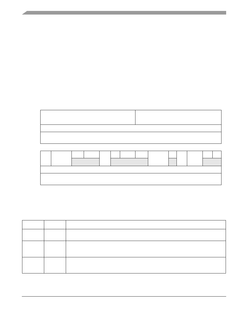
I
31
30
29
28
27
26
25
24
23
22
21
20
19
18
17
16
R
BA
ADMSK
W
Reset
0
0
0
0
0
0
0
0
0
0
0
0
0
0
0
0
Reg
Addr
ACR0: 0x004; ACR1: 0x005; ACR2: 0x006; ACR3: 0x007
15
14
13
12
11
10
9
8
7
6
5
4
3
2
1
0
R
E
S
0
0
AMM
0
0
0
CM
0
SP
W
1
0
0
W
Reset
0
0
0
0
0
0
0
0
0
0
0
0
0
0
0
0
Reg
Addr
ACR0: 0x004; ACR1: 0x005; ACR2: 0x006; ACR3: 0x007
1
Reserved in ACR2 and ACR3.
Figure 7-9. Access Control Register Format (ACRn)
Table 7-5. ACRn Field Descriptions
Bits
Name
Description
31–24
BA
Base address. Compared with address bits A[31:24]. Eligible addresses that match are assigned
the access control attributes of this register.
23–16
ADMSK
Address mask. Setting a mask bit causes the corresponding address base bit to be ignored. The
low-order mask bits can be set to define contiguous regions larger than 16 Mbytes. The mask can
define multiple noncontiguous regions of memory.
15
E
Enable. Enables or disables the other ACRn bits.
0 Access control attributes disabled
1 Access control attributes enabled