3 bypass register, 4 jtag_cfm_clkdiv register, 5 test_ctrl register – Freescale Semiconductor MCF5480 User Manual
Page 713: Bypass register -5, Jtag_cfm_clkdiv register -5, Test_ctrl register -5
Memory Map/Register Definition
MCF548x Reference Manual, Rev. 3
Freescale Semiconductor
23-5
23.3.2.3
Bypass Register
The bypass register is a single-bit shift register path from TDI to TDO when the BYPASS instruction is
selected.
23.3.2.4
JTAG_CFM_CLKDIV Register
The JTAG_CFM_CLKDIV register is a 7-bit clock divider for the CFM that is used with the
LOCKOUT_RECOVERY instruction. It controls the period of the clock used for timed events in the CFM
erase algorithm. The JTAG_CFM_CLKDIV register must be loaded before the lockout sequence can
begin.
23.3.2.5
TEST_CTRL Register
The TEST_CTRL register is a 3-bit shift register path from TDI to TDO when the
ENABLE_TEST_CTRL instruction is selected. The TEST_CTRL transfers its value to a parallel hold
register on the rising edge of TCK when the TAP state machine is in the update-DR state.
31
30
29
28
27
26
25
24
23
22
21
20
19
18
17
16
R
JTAGID
W
Reset
See
Reg
Addr
MBAR + 0x50
15
14
13
12
11
10
9
8
7
6
5
4
3
2
1
0
R
JTAGID
W
Reset
See
Reg
Addr
MBAR + 0x50
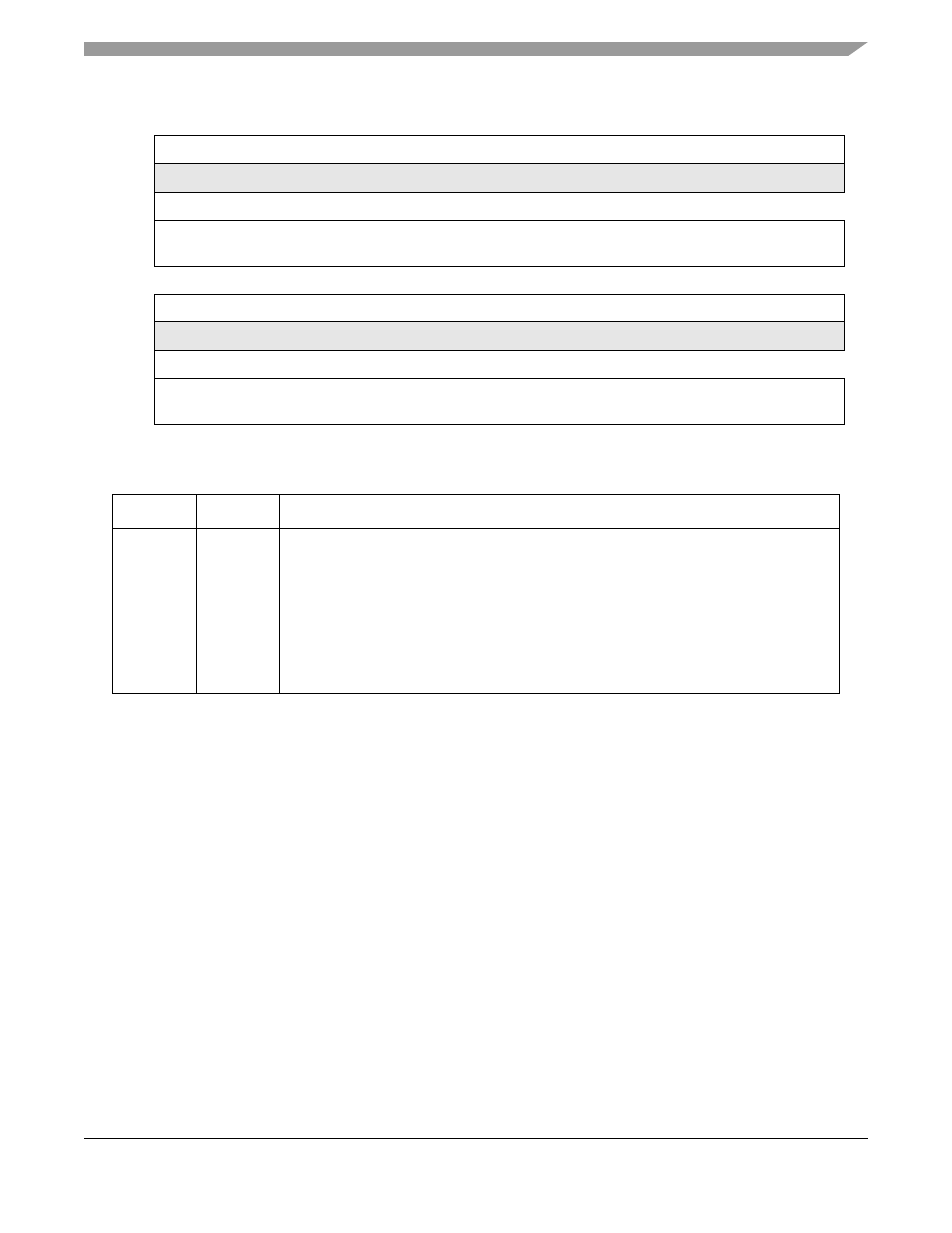
Figure 23-2. JTAG IDCODE Register
Table 23-4. JTAG IDCODE Field Descriptions
Bits
Name
Description
31–0
JTAGID
The JTAG identification number register is a read only register which contains the JTAG ID
number for the MCF548x. Its value is hard coded and cannot be modified.
Values for the MCF548x are the following:
MCF5485 0x0800c01d
MCF5484 0x0800d01d
MCF5483 0x0800e01d
MCF5482 0x0800f01d
MCF5481 0x0801001d
MCF5480 0x0801101d