17 write debug module register (wdmreg) – Freescale Semiconductor MCF5480 User Manual
Page 300
MCF548x Reference Manual, Rev. 3
8-50
Freescale Semiconductor
shows the definition of DRc encoding.
Command Sequence:
Figure 8-48.
RDMREG
Command Sequence
Operand Data:
None
Result Data:
The contents of the selected debug register are returned as a longword value. The
data is returned most-significant word first.
8.5.3.3.17
Write Debug Module Register (
WDMREG
)
The operand (longword) data is written to the specified debug module register. All 32 bits of the register
are altered by the write. DSCLK must be inactive while the debug module register writes from the CPU
accesses are performed using the WDEBUG instruction.
Command Format:
shows the definition of the DRc write encoding.
Command Sequence:
15
12
11
8
7
5
4
0
Command
0x2
0xD
100
DRc
Result
D[31:16]
D[15:0]
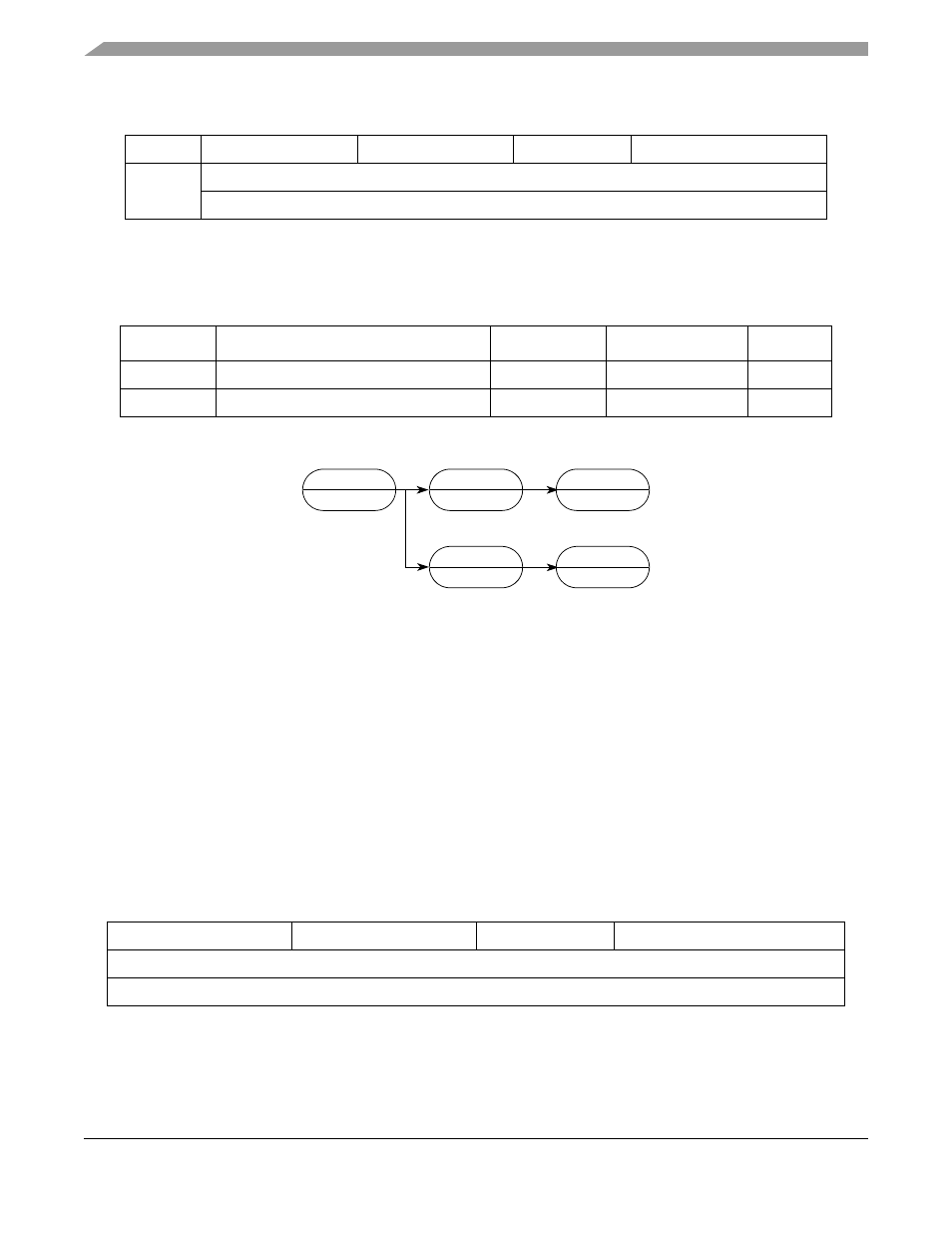
Figure 8-47.
RDMREG
BDM
Command/Result Formats
Table 8-27. Definition of DRc Encoding—Read
DRc[4:0]
Debug Register Definition
Mnemonic
Initial State
Page
0x00
Configuration/Status
CSR
0x0
0x01–0x1F
Reserved
—
—
—
Figure 8-49.
WDMREG
BDM Command Format
15
12
11
8
7
5
4
0
0x2
0xC
100
DRc
D[31:16]
D[15:0]
RDMREG
???
XXX
MS RESULT
NEXT CMD
LS RESULT
XXX
’ILLEGAL’
NEXT CMD
’NOT READY’