Freescale Semiconductor MCF5480 User Manual
Page 223
SRAM Register Definition
MCF548x Reference Manual, Rev. 3
Freescale Semiconductor
7-3
RAMBARn fields are described in detail in
.
31
30
29
28
27
26
25
24
23
22
21
20
19
18
17
16
R
BA
W
Reset
0
0
0
0
0
0
0
0
0
0
0
0
0
0
0
0
15
14
13
12
11
10
9
8
7
6
5
4
3
2
1
0
R
BA
0
0
0
WP
D/I
0
C/I
SC
SD
UC
UD
V
W
Reset
0
0
0
0
0
0
0
0
0
0
0
0
0
0
0
0
Reg
Addr
CPU space + 0xC04 (RAMBAR0), 0xC05 (RAMBAR1)
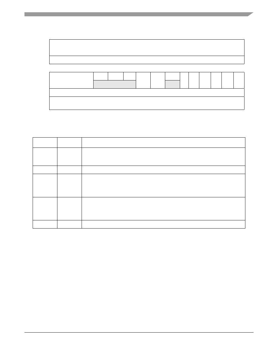
Figure 7-1. SRAM Base Address Registers (RAMBARn)
Table 7-1. RAMBARn Field Description
Bits
Name
Description
31–12
BA
Base address. Defines the SRAM module’s word-aligned base address. Each SRAM
module occupies a 4-Kbyte space defined by the contents of BA. SRAM may reside on any
4-Kbyte boundary in the 4 Gbyte address space.
11–9
—
Reserved. Should be cleared.
8
WP
Write protect. Controls read/write properties of the SRAM.
0 Allows read and write accesses to the SRAM module
1 Allows only read accesses to the SRAM module. Any attempted write reference
generates an access error exception to the ColdFire processor core.
7
D/I
Data/instruction bus. Indicates whether SRAM is connected to the internal data or
instruction bus.
0 Data bus
1 Instruction bus
6
—
Reserved, should be cleared.