3 address/data bus multiplexing, 4 bus cycle execution, Address/data bus multiplexing -13 – Freescale Semiconductor MCF5480 User Manual
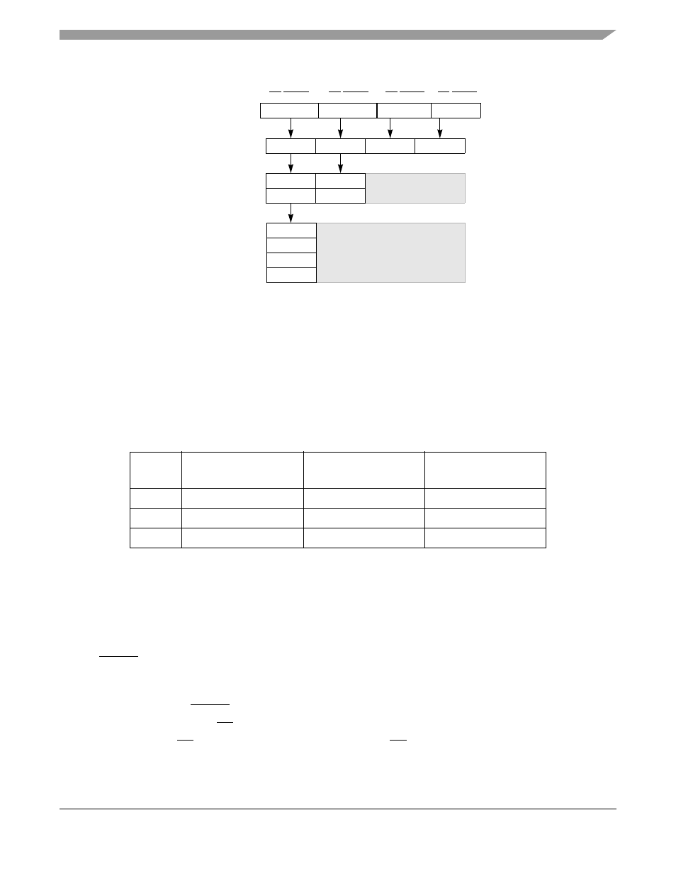
Page 429: Bus cycle execution -13, 0] to ad[31:16]. see, Figure 17-6
Functional Description
MCF548x Reference Manual, Rev. 3
Freescale Semiconductor
17-13
Figure 17-6. Connections for External Memory Port Sizes
17.6.3
Address/Data Bus Multiplexing
The MCF548x FlexBus uses a 32-bit wide multiplexed address and data bus (AD[31:0]). The full 32-bit
address will always be driven on the first clock of a bus cycle. During the data phase, which AD[31:0] lines
are used for data is determined by the programmed port size for the corresponding chip select. The
MCF548x continues to drive the address on any AD[31:0] lines that are not used for data.
lists the supported combinations of address and data bus widths.
17.6.4
Bus Cycle Execution
, basic bus operations occur in four clocks, as follows:
1. At the first clock edge, the address, attributes, and ALE are driven.
2. FBCSn is asserted at the second rising clock edge to indicate which device has been selected and
by that time the address and attributes are valid and stable. ALE is negated at this edge.
For a write transfer, data is driven on the bus at this clock edge and continues to be driven until one
clock cycle after FBCSn negates. For a read transfer, data is also returned at this cycle.
External slave asserts TA at this clock edge.
3. Read data and TA are sampled on the third clock edge. TA can be negated after this edge and read
data can then be tristated.
Table 17-10. FlexBus Operating Modes
Port Size
Address Signals During
Address Phase
Data Signals During
Data Phase
Address Signals During
Data Phase
32-bit
AD[31:0]
AD[31:0]
--
16-bit
AD[31:0]
AD[31:16]
AD[15:0]
8-bit
AD[31:0]
AD[31:24]
AD[23:0]
1
The 32-bit Address/32-bit Data non-multiplexed mode uses the PCI address/data bus to
provide a second 32-bit bus for the address. PCI cannot be used if this mode is selected.
Processor
Data Bus
Byte 0
8-Bit Port
16-Bit Port
32-Bit Port
Byte 1
Byte 2
Byte 3
Byte 0
Byte 1
Byte 2
Byte 3
Byte 0
Byte 1
Byte 2
Byte 3
AD[31:24]
AD[23:16]
AD[15:8]
AD[7:0]
External
Memory
Memory
Memory
Byte Select
Driven with
address values
Driven with
address values
BE/BWE0
BE/BWE1
BE/BWE2
BE/BWE3