3 bus cycle multiplexing, Bus cycle multiplexing -17, Figure 17-11 – Freescale Semiconductor MCF5480 User Manual
Page 433: Basic bus operations occur in
Functional Description
MCF548x Reference Manual, Rev. 3
Freescale Semiconductor
17-17
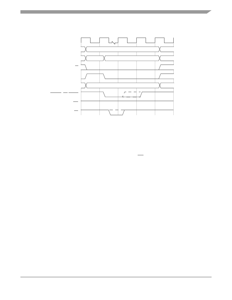
The write cycle timing diagram is shown in
Figure 17-11. Basic Write Bus Cycle
17.6.5.3
Bus Cycle Multiplexing
This section shows timing diagrams for various port size scenarios.
read transfer to a 16-bit device with no wait states. The address is driven on the full AD[31:0] bus in the
first clock. The MCF548x tristates AD[31:16] on the second clock and continues to drive address on
AD[15:0] throughout the bus cycle. The external device returns the read data on AD[31:16] and may
tristate the data line or continue to drive the data one clock after TA is sampled asserted.
CLK
AD[X:0]
AD[31:Y]
R/W
ALE
FBCSn, BE/BWEn
TA
OE
S0
S1
S2
S3
ADDR[X:0]
A[31:Y]
DATA
TSIZ[1:0]
TSIZ[1:0]