9 pci grant pin assignment register (par_pcibg), Pci grant pin assignment register (par_pcibg) -25 – Freescale Semiconductor MCF5480 User Manual
Page 397
Memory Map/Register Definition
MCF548x Reference Manual, Rev. 3
Freescale Semiconductor
15-25
15.3.2.9
PCI Grant Pin Assignment Register (PAR_PCIBG)
The PAR_PCIBG register controls the functions of the PCI grant pins. The PAR_PCIBG register is
read/write.
3
PAR_SDA
SDA Pin Assignment. Configures the SDA pin for its primary function or general purpose I/O.
0 SDA pin configured for general purpose input (PFECI2C1)
1 SDA pin configured for SDA function
2
PAR_SCL
SCL Pin Assignment. Configures the SCL pin for its primary function or general purpose I/O.
0 SCL pin configured for GPIO (PFECI2C0)
1 SCL pin configured for SCL function
1
PAR_
IRQ6
IRQ6 Pin Assignment. Configures the IRQ6 pin for one of its primary functions.
0 IRQ6 pin configured for FlexCAN CANRX1
1 IRQ6 pin configured for IRQ6 function
Note that GPIO is obtained on the IRQ6 pin by (1) writing a 1 to PAR_IRQ6 and (2) disabling the
IRQ6 function in the EPORT module.
0
PAR_
IRQ5
IRQ5 Pin Assignment. Configures the IRQ5 pin for one of its primary functions.
0 IRQ5 pin configured for FlexCAN CANRX1
1 IRQ5 pin configured for IRQ5 function
Note that GPIO is obtained on the IRQ5 pin by (1) writing a 1 to PAR_IRQ5 and (2) disabling the
IRQ5 function in the EPORT module.
15
14
13
12
11
10
9
8
7
6
5
4
3
2
1
0
R
0
0
0
0
0
0
PAR_
PCIBG4
PAR_
PCIBG3
PAR_
PCIBG2
PAR_
PCIBG1
PAR_
PCIBG0
W
Reset
0
0
0
0
0
0
0
0
0
0
0
0
0
0
0
0
Reg
Addr
MBAR + 0xA48 (PAR_PCIBG)
Figure 15-26. PCI Grant Pin Assignment Register (PAR_PCIBG)
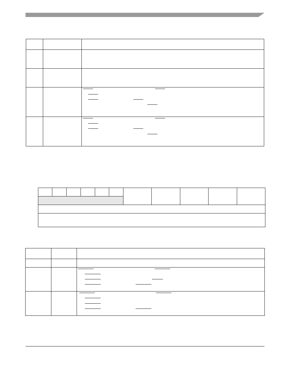
Table 15-28. PAR_PCIBG Field Descriptions
Bits
Name Description
15–10
—
Reserved, should be cleared.
9–8
PAR_
PCIBG4
PCIBG4 pin assignment. Configures the PCIBG4 pin for one of its primary functions or GPIO.
0X PCIBG4 pin configured for general purpose I/O (PPCIGNT4)
10 PCIBG4 pin configured for FlexBus TBST function
11 PCIBG4 pin configured for PCIBG4 function
7–6
PAR_
PCIBG3
PCIBG3 pin assignment. Configures the PCIBG3 pin for one of its primary functions or GPIO.
0X PCIBG3 pin configured for general purpose I/O (PPCIGNT3)
10 PCIBG3 pin configured for GP timer TOUT3 function
11 PCIBG3 pin configured for PCIBG3 function
Table 15-27. PAR_FEC/I2C/IRQ Field Descriptions (Continued)
Bits
Name Description