4 dspi serial input (dspisin), 5 dspi serial output (dspisout), 6 dspi serial clock (dspisck) – Freescale Semiconductor MCF5480 User Manual
Page 822: 6 memory map and registers, Dspi serial input (dspisin) -4, Dspi serial output (dspisout) -4, Dspi serial clock (dspisck) -4, Memory map and registers -4
MCF548x Reference Manual, Rev. 3
27-4
Freescale Semiconductor
27.5.2.4
DSPI Serial Input (DSPISIN)
DSPISIN is a serial data input signal.
27.5.2.5
DSPI Serial Output (DSPISOUT)
DSPISOUT is a serial data output signal.
27.5.2.6
DSPI Serial Clock (DSPISCK)
DSPISCK is a synchronous serial communication clock signal. In master mode, the DSPI generates the
DSPISCK. In slave mode, DSPISCK is an input from an external bus master.
27.6
Memory Map and Registers
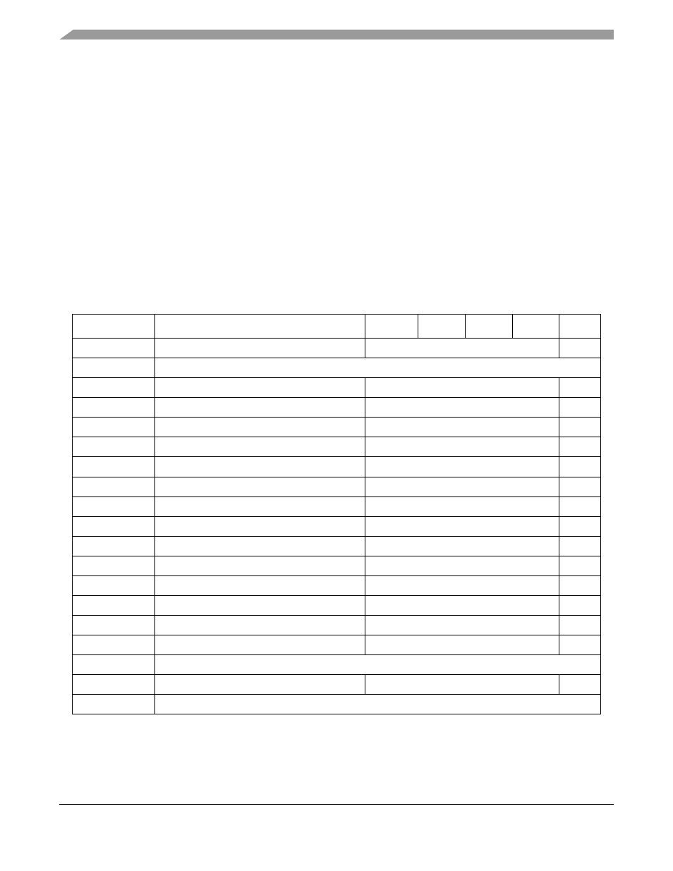
shows the DSPI memory map.
Table 27-2. DSPI Memory Map
MBAR Offset
Name
Byte0
Byte1
Byte2
Byte3
Access
0x8A00
DSPI Module Configuration Register
DMCR
R/W
0x8A04
Reserved
0x8A08
DSPI Transfer Count Register
DTCR
R/W
0x8A0C
DSPI Clock and Transfer Attributes Register 0
DCTAR0
R/W
0x8A10
DSPI Clock and Transfer Attributes Register 1
DCTAR1
R/W
0x8A14
DSPI Clock and Transfer Attributes Register 2
DCTAR2
R/W
0x8A18
DSPI Clock and Transfer Attributes Register 3
DCTAR3
R/W
0x8A1C
DSPI Clock and Transfer Attributes Register 4
DCTAR4
R/W
0x8A20
DSPI Clock and Transfer Attributes Register 5
DCTAR5
R/W
0x8A24
DSPI Clock and Transfer Attributes Register 6
DCTAR6
R/W
0x8A28
DSPI Clock and Transfer Attributes Register 7
DCTAR7
R/W
0x8A2C
DSPI Status Register
DSR
R
0x8A30
DSPI DMA/Interrupt Request Select Register
DIRSR
R/W
0x8A34
DSPI Tx FIFO Register
DTFR
R/W
0x8A38
DSPI Rx FIFO Register
DRFR
R/W
0x8A3C–0x8A48
DSPI Tx FIFO Debug Registers
DTFDRn
R
0x8A4C–0x8A78
Reserved
0x8A7C–0x8A88
DSPI Rx FIFO Debug Registers
DRFDRn
R
0x8A8C–0x8AB8
Reserved