Freescale Semiconductor MCF5480 User Manual
Page 378
MCF548x Reference Manual, Rev. 3
15-6
Freescale Semiconductor
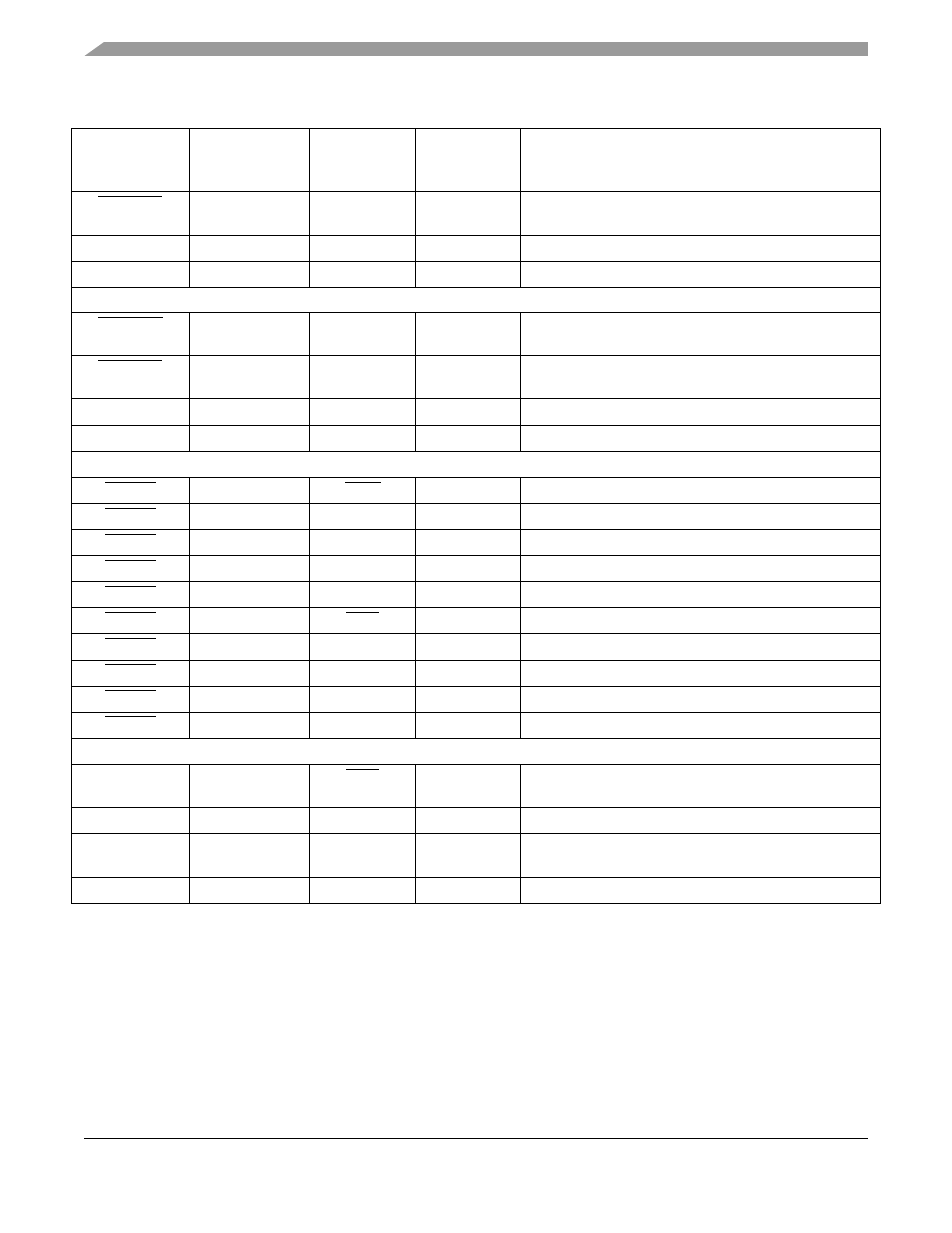
Refer to the signals chapter of the MCF548x chip specification for more detailed descriptions of these
signals. The function of most of the pins (primary function, GPIO, etc.) is determined by the GPIO module
pin assignment registers.
PSC1RTS
PPSC1PSC06
PSC1FSYNC
—
PSC1 request-to-send indication / Port PSC1PSC06 /
PSC1 frame sync
PSC1RXD
PPSC1PSC05
—
—
PSC1 receive data / Port PSC1PSC05
PSC1TXD
PPSC1PSC04
—
—
PSC1 transmit data / Port PSC1PSC04
Programmable Serial Control Module 0
PSC0CTS
PPSC1PSC03
PSC0BCLK
—
PSC0 clear-to-send indication / Port PSC1PSC03 / PSC0
modem clock
PSC0RTS
PPSC1PSC02
PSC0FSYNC
—
PSC0 request-to-send indication / Port PSC1PSC02 /
PSC0 frame sync
PSC0RXD
PPSC1PSC01
—
—
PSC0 receive data / Port PSC1PSC01
PSC0TXD
PPSC1PSC00
—
—
PSC0 transmit data / Port PSC1PSC00
Peripheral Component Interface
PCIBG4
PPCIGNT4
TBST
—
PCI bus grant 4 / Port PCIGNT4 / Flexbus transfer burst
PCIBG3
PPCIGNT3
TOUT3
—
PCI bus grant 3 / Port PCIGNT3 / GP timer out 3
PCIBG2
PPCIGNT2
TOUT2
—
PCI bus grant 2 / Port PCIGNT2 / GP timer out 2
PCIBG1
PPCIGNT1
TOUT1
—
PCI bus grant 1 / Port PCIGNT1 / GP timer out 1
PCIBG0
PPCIGNT0
TOUT0
—
PCI bus grant 0 / Port PCIGNT0 / GP timer out 0
PCIBR4
PPCIREQ4
IRQ4
—
PCI bus request 4 / Port PCIREQ4 / Interrupt 4
PCIBR3
PPCIREQ3
TIN2
—
PCI bus request 3 / Port PCIREQ3 / GP timer in 3
PCIBR2
PPCIREQ2
TIN2
—
PCI bus request 2 / Port PCIREQ2 / GP timer in 2
PCIBR1
PPCIREQ1
TIN1
—
PCI bus request 1 / Port PCIREQ1 / GP timer in 1
PCIBR0
PPCIREQ0
TIN0
—
PCI bus request 0 / Port PCIREQ0 / GP timer in 0
General Purpose Timer
TIN3
PTIM3
2
IRQ3
CANRX1
GP timer in 3 / Port TIM7 / Interrupt 3 / FlexCAN 1 receive
data
TOUT3
PTIM7
2
CANTX1
—
GP timer out 3 / Port TIM6 / FlexCAN 1 transmit data
TIN2
PTIM2
2
IRQ2
CANRX1
GP timer in 2 / Port TIM5 / Interrupt 1 / FlexCAN 2 receive
data
TOUT2
PTIM6
2
CANTX1
—
GP timer out 2 / Port TIM4 / FlexCAN 1 transmit data
1
The primary functionality of a pin is not necessarily the default function of the pin after reset. Most pins that have muxed GPIO
functionality will default to GPIO inputs. See the reset value of the associated pin assignment register. See
x Pin Assignment Registers (PAR_x)
”) for more information on default pin functionality.
2
GPIO is supported, but the GPIO functionality is controlled by the timer or EPORT module instead of the GPIO module. Signals
are listed because there are pin assignment registers in the GPIO module for controlling the signal functions.
Table 15-1. MCF548x GPIO Module External Pins (Continued)
Primary
Function
(Pin Name)
1
GPIO
Alternate
Function 1
Alternate
Function 2
Description