7 dma pin assignment register (par_dma), Dma pin assignment register (par_dma) -23 – Freescale Semiconductor MCF5480 User Manual
Page 395
Memory Map/Register Definition
MCF548x Reference Manual, Rev. 3
Freescale Semiconductor
15-23
15.3.2.7
DMA Pin Assignment Register (PAR_DMA)
The PAR_DMA register controls the function of the four MCF548x DMA pins.
The PAR_DMA register is read/write
15.3.2.8
FEC/I2C/IRQ Pin Assignment Register (PAR_FECI2CIRQ)
The PAR_FECI2CIRQ register controls the functions of the FEC0, FEC1, I2C, and IRQ pins. The
PAR_FECI2CIRQ register is read/write
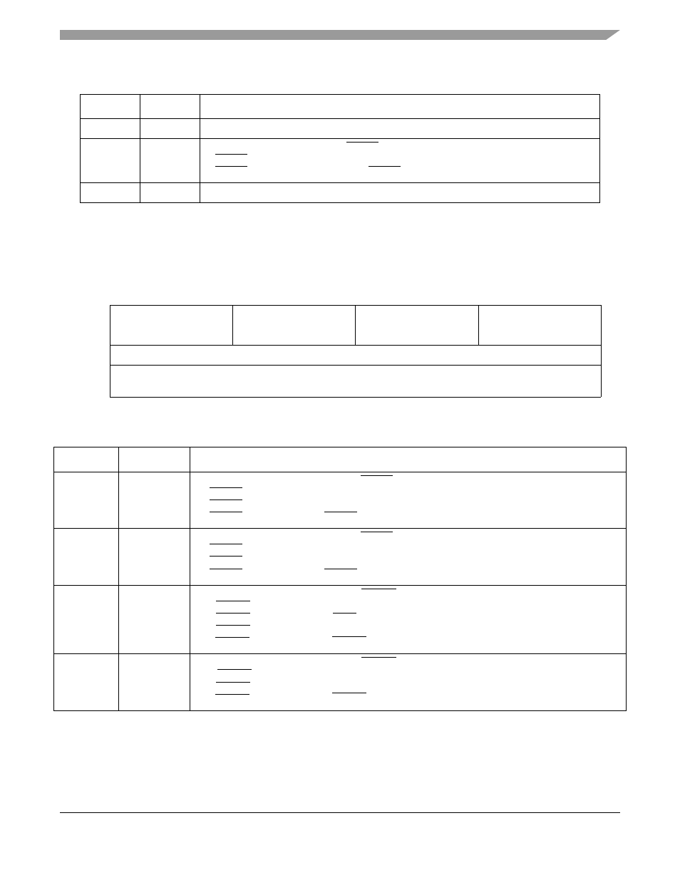
Table 15-25. PAR_FBCS Field Descriptions
Bits
Name Description
7–6
—
Reserved, should be cleared.
5–1
PAR_CSn
The PAR_CSn bit configures the FBCSn pin for its primary function or general purpose I/O.
0 FBCSn pin configured for general purpose I/O (PFBCS[5:1])
1 FBCSn pin configured for FlexBus FBCSn function
0
—
Reserved, should be cleared.
7
6
5
4
3
2
1
0
R
PAR_DACK1
PAR_DACK0
PAR_DREQ1
PAR_DREQ0
W
Reset
0
0
0
0
0
0
0
0
Reg
Addr
MBAR + 0xA43 (PAR_DMA)
Figure 15-24. DMA Pin Assignment Register (PAR_DMA)
Table 15-26. PAR_DMA Field Descriptions
Bits
Name Description
7–6
PAR_DACK1
The PAR_DACK1 field configures the DACK1 pin for its primary functions or general purpose I/O.
0X DACK1 pin configured for general purpose I/O (PDMA3)
10 DACK1 pin configured for GP Timer TOUT1 function
11 DACK1 pin configured for DACK1 function
5–4
PAR_DACK0
The PAR_DACK0 field configures the DACK0 pin for its primary functions or general purpose I/O.
0X DACK0 pin configured for general purpose I/O (PDMA2)
10 DACK0 pin configured for GP Timer TOUT0 function
11 DACK0 pin configured for DACK0 function
3–2
PAR_DREQ1 The PAR_DREQ1 field configures the DREQ1 pin for its primary functions or general purpose I/O.
00 = DREQ1 pin configured for general purpose I/O (PDMA1)
01 = DREQ1 pin configured for IRQ1 function
10 = DREQ1 pin configured for GP Timer TIN1 function
11 = DREQ1 pin configured for DREQ1 function
1–0
PAR_DREQ0 The PAR_DREQ0 field configures the DREQ0 pin for its primary functions or general purpose I/O.
0X = DREQ0 pin configured for general purpose I/O (PDMA0)
10 = DREQ0 pin configured for GP Timer TIN0 function
11 = DREQ0 pin configured for DREQ0 function