4 sdram configuration 2 register settings, 5 sdram control register settings and pall command, Sdram configuration 2 register settings -27 – Freescale Semiconductor MCF5480 User Manual
Page 475
SDRAM Example
MCF548x Reference Manual, Rev. 3
Freescale Semiconductor
18-27
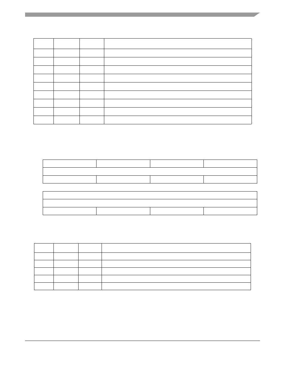
18.8.4
SDRAM Configuration 2 Register Settings
The SDCFG2 register should be programmed as shown in
.
This configuration results in a value of SDCFG2 = 0x4677_0000, as described in
18.8.5
SDRAM Control Register Settings and PALL command
The SDCR should be programmed as shown in
. Along with the base settings for the SDCR
the MODE_EN and IPALL bits are set to issue a PALL command to the SDRAM and enable writing of
the mode register.
23–20
RDLAT
0110
0x6 is the recommended value for DDR memory with a CASL of 2
19
—
0
Reserved. Should be cleared.
18–16
ACT2RW
010
ACT2RW = t
RCD
/SDCLK - 1 = 18ns/8.3ns - 1 = 2.16 - 1 = 1.16, rounded up to 2
15
—
0
Reserved. Should be cleared.
14–12
PRE2ACT
010
PRE2ACT = t
RP
/SDCLK - 1 = 18ns/8.3ns - 1 = 2.16 - 1 = 1.16, rounded up to 2
11–8
REF2ACT
1000
REF2ACT = t
RFC
/SDCLK - 1 = 75ns/8.3ns - 1 = 9 - 1 = 8
7
—
0
Reserved. Should be cleared.
6–4
WTLAT
011
0x3 is the recommended value for DDR
3–0
CSSZ
1101
Total size is 64 Mbytes. 2 x 256Mbit = 64Mbytes
31
30
29
28
27
26
25
24
23
22
21
20
19
18
17
16
Field
BRD2PRE
BWT2RW
BRD2WT
BL
Setting
0100
_
0110
_
0111
_
0111
(hex)
4
6
7
7
15
14
13
12
11
10
9
8
7
6
5
4
3
2
1
0
Field
—
Setting
0000_0000_0000_0000
(hex)
0
0
0
0
Figure 18-17. SDRAM Example Configuration Register 2 Settings (SDCFG2)
Table 18-18. SDCFG2 Field Descriptions
Bits
Name
Setting
Description
31–28
BRD2PRE
0100
BRD2PRE = burst length/2 = 8/2 = 4
27–24
BWT2RW
0110
BWT2RW = burst length/2 + t
WR
= 8/2 + 2 = 4 + 2 =
6
23–20
BRD2WT
0111
0x7 is the recommended value for DDR
19–16
BL
0111
BL = burst length - 1 = 8 - 1 =
7
15–0
—
0
Reserved. Should be cleared.
Table 18-17. SDCFG1 Field Descriptions (Continued)
Bits
Name
Setting
Description