11 enable automatic refresh and lock mode register – Freescale Semiconductor MCF5480 User Manual
Page 481
SDRAM Example
MCF548x Reference Manual, Rev. 3
Freescale Semiconductor
18-33
18.8.11 Enable Automatic Refresh and Lock Mode Register
The SDCR should be programmed as shown in
. Along with the base settings for the SDCR
the REF bit is set to enable automatic refreshing of the memory. In addition, the MODE_EN bit is cleared
to disable write to the SDMR.
This configuration results in a value of SDCR = 0x710D_0F00, as described in
.
21
BT
0
Sequential burst type.
20–18
BLEN
011
Burst length of eight.
17
—
0
Reserved. Should be cleared.
16
CMD
1
Initiate the LMR command.
15–0
—
0
Reserved. Should be cleared.
31
30
29
28
27
26
25
24
23
22
21
20
19
18
17
16
Field MODE
_EN
CKE
DDR
REF
—
MUX
AP
DRIV
E
RCNT
Setting
0111_0001_0000_1101
(hex)
7
1
0
D
15
14
13
12
11
10
9
8
7
6
5
4
3
2
1
0
Field
—
DQS_OE
—
BUFF
—
IREF IPALL
—
Setting
0000_1111_0000_0000
(hex)
0
F
0
0
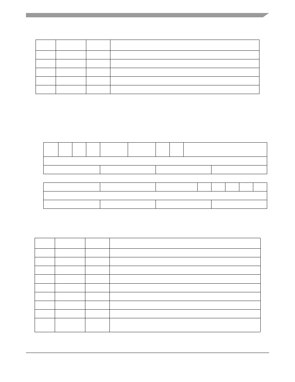
Figure 18-24. SDRAM Control Register Settings + REF
Table 18-25. SDCR + REF Field Descriptions
Bits
Name
Setting
Description
31
MODE_EN
0
Mode register is not writable.
30
CKE
1
SDCKE is asserted
29
DDR
1
DDR mode is enabled
28
REF
1
Automatic refresh is enabled.
27–26
—
00
Reserved. Should be cleared.
25–24
MUX
01
01 is the MUX setting for a 13 x 9 x 4 memory. See
.
23
AP
0
0 sets the auto precharge control bit to A10.
22
DRIVE
0
Data and DQS lines are only driven for a write cycle.
21–16
RCNT
001101
RCNT = (t
REFI
/ (SDCLK x 64)) - 1 = (7800ns/(8.3ns x 64)) - 1 = 13.62, round
down to 13 (0xD)
Table 18-24. SDMR Field Descriptions (Continued)
Bits
Name
Setting
Description