16 read debug module register (rdmreg), Command sequence – Freescale Semiconductor MCF5480 User Manual
Page 299
Background Debug Mode (BDM)
MCF548x Reference Manual, Rev. 3
Freescale Semiconductor
8-49
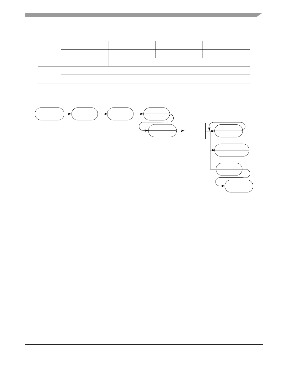
Command Sequence:
Figure 8-46.
WCREG
Command Sequence
Operand Data:
This instruction requires two longword operands. The first selects the register to
which the operand data is to be written; the second contains the data.
Result Data:
Successful write operations return 0xFFFF. Bus errors on the write cycle are
indicated by the setting of bit 16 in the status message and by a data pattern of
0x0001.
8.5.3.3.16
Read Debug Module Register (
RDMREG
)
Read the selected debug module register and return the 32-bit result. The only valid register selection for
the
RDMREG
command is CSR (DRc = 0x00). Note that this read of the CSR clears the trigger status bits
(CSR[BSTAT]) if either a level-2 breakpoint has been triggered or a level-1 breakpoint has been triggered
and no level-2 breakpoint has been enabled.
Command/Result Formats:
15
12
11
8
7
4
3
0
Command
0x2
0x8
0x8
0x0
0x0
0x0
0x0
0x0
0x0
Rc
Result
D[31:16]
D[15:0]
Figure 8-45.
WCREG
Command/Result Formats
XXX
’NOT READY’
WCREG
???
MS ADDR
’NOT READY’
MS ADDR
’NOT READY’
WRITE
CONTROL
REGISTER
NEXT CMD
’CMD COMPLETE’
MS DATA
’NOT READY’
NEXT CMD
’NOT READY’
XXX
BERR
LS DATA
’NOT READY’