10 pci request pin assignment register (par_pcibr) – Freescale Semiconductor MCF5480 User Manual
Page 398
MCF548x Reference Manual, Rev. 3
15-26
Freescale Semiconductor
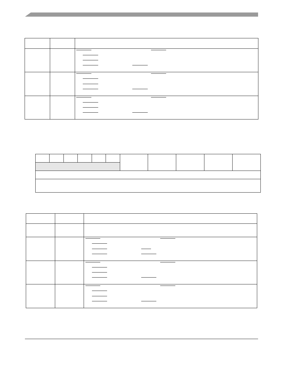
15.3.2.10 PCI Request Pin Assignment Register (PAR_PCIBR)
The PAR_PCIBR controls the functions of the PCI request pins. The PAR_PCIBR is read/write.
5–4
PAR_
PCIBG2
PCIBG2 pin assignment. Configures the PCIBG2 pin for one of its primary functions or GPIO.
0X PCIBG2 pin configured for general purpose I/O (PPCIGNT2)
10 PCIBG2 pin configured for GP timer TOUT2 function
11 PCIBG2 pin configured for PCIBG2 function
3–2
PAR_
PCIBG1
PCIBG1 pin assignment. Configures the PCIBG1 pin for one of its primary functions or GPIO.
0X PCIBG1 pin configured for general purpose I/O (PPCIGNT1)
10 PCIBG1 pin configured for GP timer TOUT1 function
11 PCIBG1 pin configured for PCIBG1 function
1–0
PAR_
PCIBG0
PCIBG0 pin assignment. Configures the PCIBG0 pin for one of its primary functions or GPIO.
0X PCIBG0 pin configured for general purpose I/O (PPCIGNT0)
10 PCIBG0 pin configured for GP timer TOUT0 function
11 PCIBG0 pin configured for PCIBG0 function
15
14
13
12
11
10
9
8
7
6
5
4
3
2
1
0
R
0
0
0
0
0
0
PAR_PCIBR4 PAR_PCIBR3 PAR_PCIBR2 PAR_PCIBR1 PAR_PCIBR0
W
Reset
0
0
0
0
0
0
0
0
0
0
0
0
0
0
0
0
Reg
Addr
MBAR + 0xA4A (PAR_PCIBR)
Figure 15-27. PCI Request Pin Assignment Register (PAR_PCIBR)
Table 15-29. PAR_PCIBR Field Descriptions
Bits
Name
Description
15–10
—
Reserved, should be cleared. Writes have no effect and terminate without transfer error
exception
9–8
PAR_PCIBR4 PCIBR4 Pin Assignment. Configures the PCIBR4 pin for one of its primary functions or GPIO.
0X PCIBR4 pin configured for general purpose I/O (PPCIREQ4)
10 PCIBR4 pin configured for IRQ4 function
11 PCIBR4 pin configured for PCIBR4 function
7–6
PAR_PCIBR3 PCIBR3 Pin Assignment. Configures the PCIBR3 pin for one of its primary functions or GPIO.
0X PCIBR3 pin configured for general purpose I/O (PPCIREQ3)
10 PCIBR3 pin configured for GP timer TIN3 function
11 PCIBR3 pin configured for PCIBR3 function
5–4
PAR_PCIBR2 PCIBR2 Pin Assignment. Configures the PCIBR2 pin for one of its primary functions or GPIO.
0X PCIBR2 pin configured for general purpose I/O (PPCIREQ2)
10 PCIBR2 pin configured for GP timer TIN2 function
11 PCIBR2 pin configured for PCIBR2 function
Table 15-28. PAR_PCIBG Field Descriptions (Continued)
Bits
Name Description