8 issue a pall command, Issue a pall command -30, Table 18-21 – Freescale Semiconductor MCF5480 User Manual
Page 478
MCF548x Reference Manual, Rev. 3
18-30
Freescale Semiconductor
18.8.8
Issue a PALL command
The SDCR should be programmed as shown in
. This will issue a second PALL command to
the memory. The same SDCR value calculated in
Section 18.8.5, “SDRAM Control Register Settings and
This configuration results in a value of SDCR = 0xE10D_0002, as described in
.
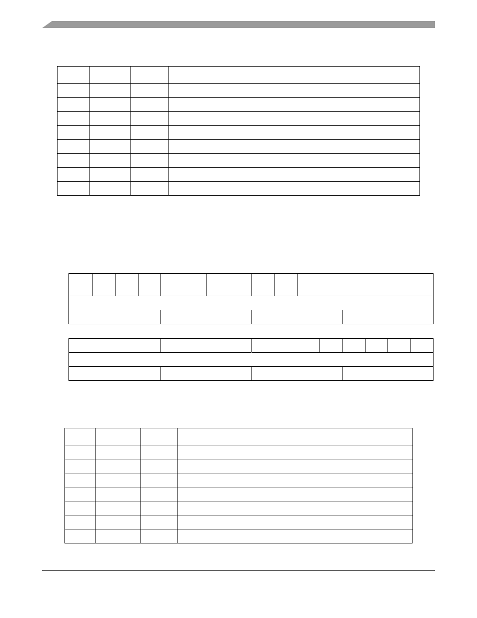
Table 18-21. SDMR Field Descriptions
Bits
Name
Setting
Description
31–30
BNKAD
00
00 selects the mode register.
29–25
OP_MODE
0010
Selects normal operating mode and resets the DLL.
24–22
CASL
010
CAS latency of two clocks.
21
BT
0
Sequential burst type.
20–18
BLEN
011
Burst length of eight
17
—
0
Reserved. Should be cleared.
16
CMD
1
Initiate the LMR command.
15–0
—
0
Reserved. Should be cleared.
31
30
29
28
27
26
25
24
23
22
21
20
19
18
17
16
Field MODE
_EN
CKE
DDR
REF
—
MUX
AP
DRIV
E
RCNT
Setting
1110_0001_0000_1101
(hex)
E
1
0
D
15
14
13
12
11
10
9
8
7
6
5
4
3
2
1
0
Field
—
DQS_OE
—
BUFF
—
IREF IPALL
—
Setting
0000_0000_0000_0010
(hex)
0
0
0
2
Figure 18-21. SDRAM Control Register Settings + MODE_EN and IPALL
Table 18-22. SDCR + MODE_EN and IPALL Field Descriptions
Bits
Name
Setting
Description
31
MODE_EN
1
Mode register is writable.
30
CKE
1
SDCKE is asserted
29
DDR
1
DDR mode is enabled
28
REF
0
Automatic refresh is disabled
27–26
—
00
Reserved. Should be cleared.
25–24
MUX
01
01 is the MUX setting for a 13 x 9 x 4 memory. See
.
23
AP
0
0 sets the auto precharge control bit to A10.