3 memory map/register definition, 1 register overview, Memory map/register definition -7 – Freescale Semiconductor MCF5480 User Manual
Page 379: Register overview -7
Memory Map/Register Definition
MCF548x Reference Manual, Rev. 3
Freescale Semiconductor
15-7
that there are several cases where a function is mapped to more than
one pin. While it is possible to enable the function on more than one pin simultaneously, this type of
programming should be avoided for input functions to prevent unexpected behavior. All multiple-pin
15.3
Memory Map/Register Definition
15.3.1
Register Overview
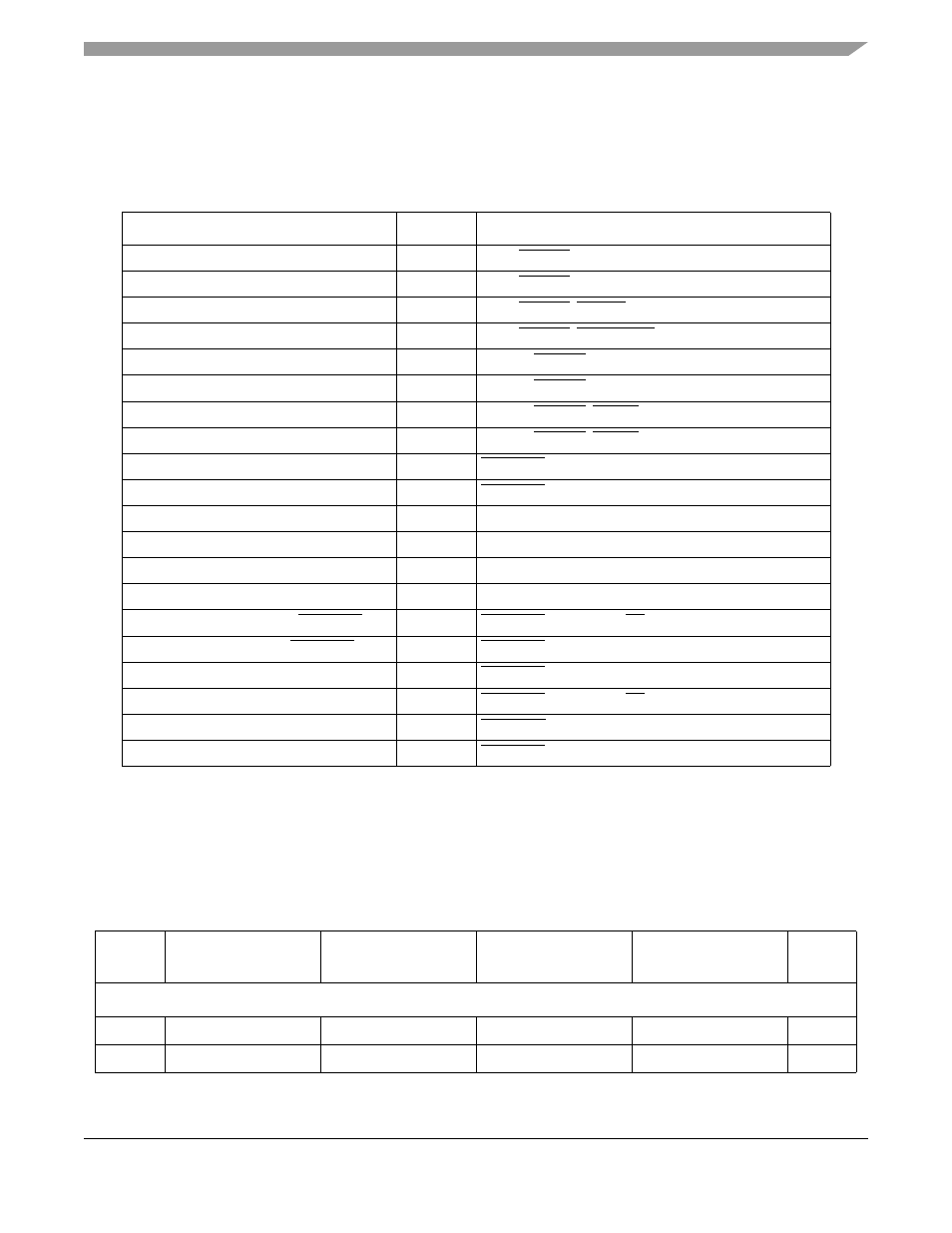
summarizes all the registers in the MCF548x GPIO module address space.
Table 15-2. MCF548x Multiple-Pin Functions
Function
Direction
Associated Pins
GP timer in 3 (TIN3)
I
TIN3, PCIBR3
GP timer in 2 (TIN2)
I
TIN2, PCIBR2
GP timer in 1 (TIN1)
I
TIN1, PCIBR1, DREQ1
GP timer in 0 (TIN0)
I
TIN0, PCIBR0, DMA_REQ0
GP timer out 3 (TOUT3)
O
TOUT3, PCIBG3, DSPI_PSC3
GP timer out 2 (T2OUT)
O
TOUT2, PCIBG2, DSPI_PSC2
GP timer out 1 (T1OUT)
O
TOUT1, PCIBG1, DACK1
GP timer out 0 (T0OUT)
O
TOUT0, PCIBG0, DACK0
FlexCAN 0 transmit data (CANTX0)
O
PSC2RTS, FEC1MDC
FlexCAN 0 receive data (CANRX0)
I
PSC2CTS, FEC1MDIO
FlexCAN 1 transmit data (CANTX1)
O
T3OUT, T2OUT, DSPI_PCS3, DSPI_PCS2
FlexCAN 1 receive data (CANRX1)
I
T3IN, T2IN, IRQ6, IRQ5
I
2
C serial data (SDA)
I/O
SDA, FEC1MDC
I
2
C serial clock (SCL)
I/O
SDA, FEC1MDIO
PSC3 request-to-send (PSC3RTS)
O
PSC3RTS, DSPIPCS0/SS
PSC3 clear-to-send (PSC3CTS)
I
PSC3CTS, DSPISCK
PSC3 modem clock (PSC3BCLK)
I
PSC3CTS, DSPISCK
PSC3 frame sync (PSC3FSYNC)
I
PSC3CTS, DSPIPCS0/SS
PSC3 uart receive data (PSC3RXD)
I
PSC3RXD, DSPISIN
PSC3 uart transmit data (PSC3TXD)
O
PSC3TXD, DSPISOUT
Table 15-3. MCF548x GPIO Module Memory Map
MBAR
Offset
31–24
23–16
15–8
7–0
Access
1
Port Output Data Registers
0xA00
PODR_FBCTL
PODR_FBCS
PODR_DMA
Reserved
3
S/U
0xA04
PODR_FEC0H
PODR_FEC0L
PODR_FEC1H
PODR_FEC1L
S/U