Chapter 23 ieee 1149.1 test access port (jtag), 1 introduction, 1 block diagram – Freescale Semiconductor MCF5480 User Manual
Page 709: Chapter 23, Ieee 1149.1 test access port (jtag), Introduction -1, Block diagram -1, Chapter 23, “ieee 1149.1 test access port (jtag)
MCF548x Reference Manual, Rev. 3
Freescale Semiconductor
23-1
Chapter 23
IEEE 1149.1 Test Access Port (JTAG)
23.1
Introduction
The Joint Test Action Group, or JTAG, is a dedicated user-accessible test logic, that complies with the
IEEE 1149.1 standard for boundary-scan testability, to help with system diagnostic and manufacturing
testing.
This architecture provides access to all data and chip control pins from the board-edge connector through
the standard four-pin test access port (TAP) and the JTAG reset pin, TRST.
23.1.1
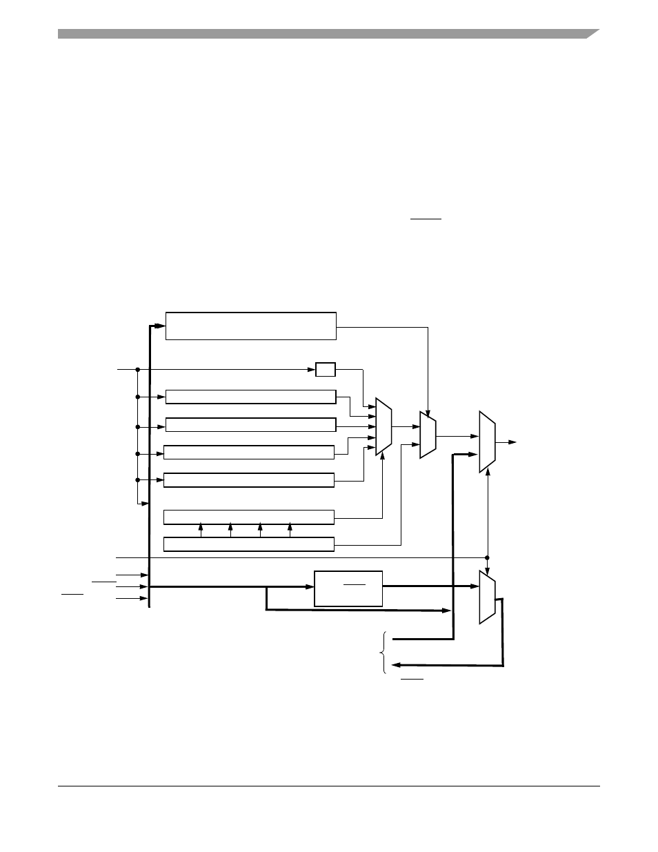
Block Diagram
shows the block diagram of the JTAG module.
Figure 23-1. JTAG Block Diagram
4-BIT TAP INSTRUCTION REGISTER
3
0
1-BIT BYPASS REGISTER
148-BIT BOUNDARY SCAN REGISTER
32-BIT IDCODE REGISTER
TRST/DSCLK
TCK
TMS/BKPT
0
31
0
147
TAP CONTROLLER
TDI/DSI
1
0
TDO/DSO
JTAG Module
to Debug Module
7-BIT JTAG_CFM_CLKDIV REGISTER
0
6
3-BIT TEST_CTRL REGISTER
0
2
4-BIT TAP INSTRUCTION DECODER
1
0
Disable DSCLK
Force BKPT = 1
DSI = 0
MTMOD0
DSO
DSI
BKPT
DSCLK