5 command register (psccrn), Command register (psccrn) -11, 5 command register (psccr n ) – Freescale Semiconductor MCF5480 User Manual
Page 773
Memory Map/Register Definition
MCF548x Reference Manual, Rev. 3
Freescale Semiconductor
26-11
The upper 4 bits set the receiver and the lower 4 bits set the transmitter clock source. To use the system
bus clock for both the transmitter and receiver, program the PSCCSR with 0xDD. It is possible to program
the transmitter and the receiver with different clock sources.
26.3.3.5
Command Register (PSCCRn)
The PSCCR is used to supply commands to the PSC. Multiple commands can be specified in a single write
to the PSCCR if the commands are not conflicting. For example, reset transmitter and enable transmitter
commands cannot be specified in a single command.
7
6
5
4
3
2
1
0
R
W
RCSEL
TCSEL
Reset
1
1
0
1
1
1
0
1
Reg
Addr
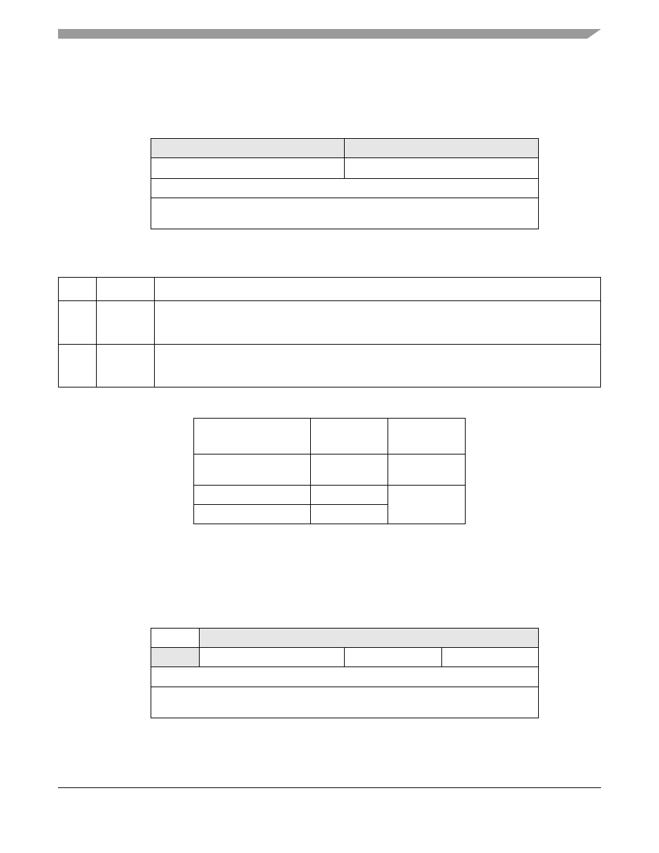
MBAR + 0x8604 (PSC0); 0x8704 (PSC1); 0x8804 (PSC2); 0x8904 (PSC3)
Figure 26-6. Clock Select Register (PSCCSRn)
Figure 26-7. PSCCSRn Field Descriptions
Bits
Name
Description
7–4
RCSEL
In UART or SIR mode, this is the receiver clock select.
shows the bit settings for this field.
In all other modes, this field is reserved.
3–0
TCSEL
In UART or SIR mode, this is the transmitter clock select.
shows the bit settings for this field.
In all other modes, this field is reserved.
Table 26-6. RCSEL[3:0] and TCSEL[3:0]
RCSEL[3:0] or
TCSEL[3:0]
UART Mode
SIR Mode
0000 – 1101
System Bus
Clock
System Bus
Clock
1110
× 16 CTM clock
× 16 CTM clock
1111
× 1 CTM clock
7
6
5
4
3
2
1
0
R
0
W
MISC
TXC
RXC
Reset
0
0
0
0
0
0
0
0
Reg
Addr
MBAR + 0x8608 (PSC0); 0x8708 (PSC1); 0x8808(PSC2); 0x8908 (PSC3)
Figure 26-8. PSC Command Register (PSCCRn)