3 cache control register (cacr), 4 access control registers (acr0-acr3), 5 ram base address registers (rambar0 and rambar1) – Freescale Semiconductor MCF5480 User Manual
Page 117: 6 module base address register (mbar), 6 programming model table, Cache control register (cacr) -13, Access control registers (acr0–acr3) -13, Module base address register (mbar) -13, Programming model table -13, 4 access control registers (acr0–acr3)
Programming Model
MCF548x Reference Manual, Rev. 3
Freescale Semiconductor
3-13
3.3.5.3
Cache Control Register (CACR)
The CACR controls operation of both the instruction and data cache memory. It includes bits for enabling,
freezing, and invalidating cache contents. It also includes bits for defining the default cache mode and
Section 7.10.1, “Cache Control Register (CACR).”
3.3.5.4
Access Control Registers (ACR0–ACR3)
The access control registers (ACR0–ACR3) define attributes for four user-defined memory regions: ACR0
and ACR1 control data memory space, and ACR2 and ACR3 control instruction memory space. Attributes
include definition of cache mode, write protect and buffer write enables. See
Control Registers (ACR0–ACR3).”
3.3.5.5
RAM Base Address Registers (RAMBAR0 and RAMBAR1)
The RAMBAR registers determine the base address location of the internal SRAM modules and indicate
the types of references mapped to each. Each RAMBAR includes a base address, write-protect bit, address
space mask bits, and an enable. The RAM base address must be aligned on a 0-module-2-Kbyte boundary.
See
Section 7.4.1, “SRAM Base Address Registers (RAMBAR0/RAMBAR1).”
3.3.5.6
Module Base Address Register (MBAR)
The module base address register (MBAR) defines the logical base address for the memory-mapped space
containing the control registers for the on-chip peripherals. See
Section 9.3.1, “Module Base Address
3.3.6
Programming Model Table
lists register names, the CPU space location, whether the register is written from the processor
using the MOVEC instruction, and the complete register name.
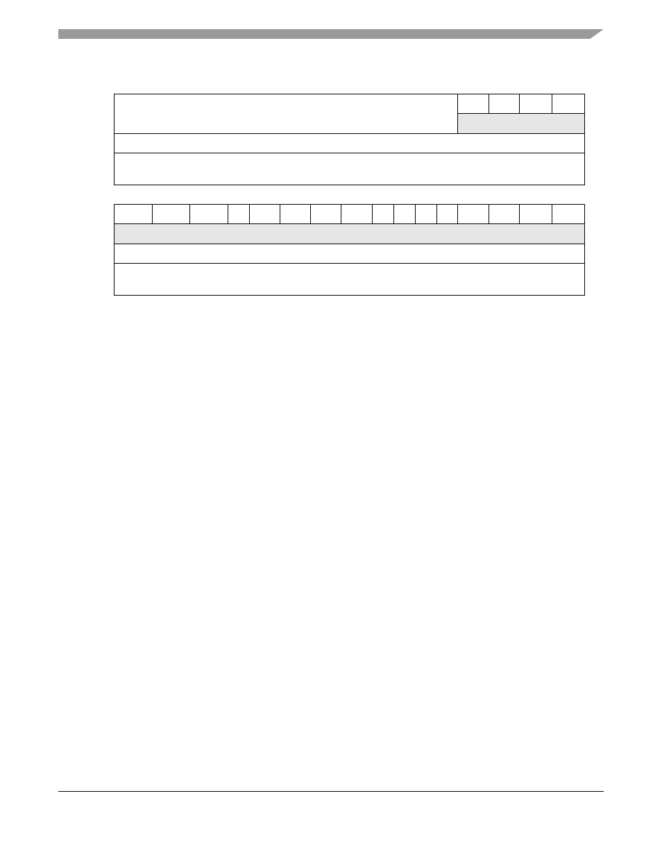
31
30
29
28
27
26
25
24
23
22
21
20
19
18
17
16
R
Exception vector table base address
1
0
0
0
0
W
Reset
0
0
0
0
0
0
0
0
0
0
0
0
0
0
0
0
Reg
Addr
0x801
15
14
13
12
11
10
9
8
7
6
5
4
3
2
1
0
R
0
0
0
0
0
0
0
0
0
0
0
0
0
0
0
0
W
Reset
0
0
0
0
0
0
0
0
0
0
0
0
0
0
0
0
Reg
Addr
0x801
1
Written from a BDM serial command or from the CPU using the MOVEC instruction. VBR can be read from
the debug module only. The upper 12 bits are returned, the low-order 20 bits are undefined.
Figure 3-8. Vector Base Register (VBR)