4 byte parity checking and generation, 1 parity generation, Table 17. parity generation – Intel CONTROLLERS 413808 User Manual
Page 92: 17 parity generation

Intel
®
413808 and 413812—Address Translation Unit (PCI-X)
Intel
®
413808 and 413812 I/O Controllers in TPER Mode
Developer’s Manual
October 2007
92
Order Number: 317805-001US
2.6.4
Byte Parity Checking and Generation
The internal bus interface of the ATU supports byte-wise parity protection on the
internal bus. This includes A_PARITY[4:0] and D_PARITY[15:0] on the address bus
(A[35:0]) and the data bus (D[127:0]) respectively.
For an outbound write request (or inbound read completion) the internal bus interface
verifies the write request address parity and data parity on the data cycles.
For an inbound read completion, the internal bus interface verifies the read completion
data parity on the data cycles.
For an inbound write request, the ATU computes and appends write request address
parity and data parity data parity prior to delivering the request to the internal bus.
For an inbound read request, the internal bus interface computes and appends read
request address parity prior to delivering the request to the internal bus.
Note:
The ATU forwards data parity across to the other interface. When a data parity error
occurs on the internal bus interface, the same data issues on the PCI bus with either
bad parity or uncorrectable ECC error. For inbound transactions the bad parity or
uncorrectable ECC errors results in the ATU marking that data bad by corrupting the
parity on the internal bus.
2.6.4.1
Parity Generation
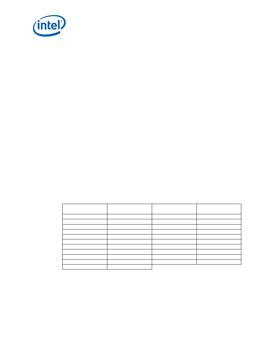
Data parity signals include byte enables in the calculation.
lists the data bits
that are used for the parity calculation. The parity bits are calculated by bit XORing the
. As an example, the parity calculation for the lowest
order byte of the data bus D[7:0] is calculated as follows:
Equation 5. D_PARITY0 = D[0] XOR D[1] XOR D[2] XOR D[3] XOR D[4] XOR D[5] XOR
D[6] XOR D[7] XOR WBE[0]
Table 17. Parity Generation
Address/Data Parity
Bit
Address/Data Bus
Address/Data Parity
Bit
Address/Data Bus
A_PARITY4
A[35:32]
D_PARITY9
D[79:72], WBE[9]
A_PARITY3
A[31:24]
D_PARITY8
D[71:64], WBE[8]
A_PARITY2
A[23:16]
D_PARITY7
D[63:56], WBE[7]
A_PARITY1
A[15:8]
D_PARITY6
D[55:48], WBE[6]
A_PARITY0
A[7:0]
D_PARITY5
D[47:40], WBE[5]
D_PARITY15
D[127:120], WBE[15]
D_PARITY4
D[39:32], WBE[4]
D_PARITY14
D[119:112], WBE[14]
D_PARITY3
D[31:24], WBE[3]
D_PARITY13
D[111:104], WBE[13]
D_PARITY2
D[23:16], WBE[2]
D_PARITY12
D[103:96], WBE[12]
D_PARITY1
D[15:8], WBE[1]
D_PARITY11
D[95:88], WBE[11]
D_PARITY0
D[7:0], WBE[0]
D_PARITY10
D[87:80], WBE[10]
