4 sram ecc log register - selogr, 4 sram ecc log register — selogr, 353 sram ecc log register — selog – Intel CONTROLLERS 413808 User Manual
Page 538: Intel, Bit default description, Upper ecc address

Intel
®
413808 and 413812—SRAM Memory Controller
Intel
®
413808 and 413812 I/O Controllers in TPER Mode
Developer’s Manual
October 2007
538
Order Number: 317805-001US
8.6.4
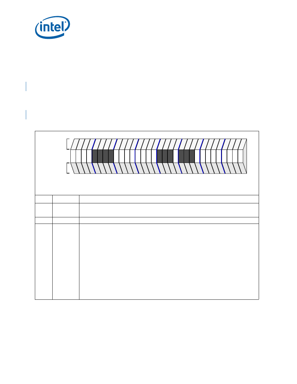
SRAM ECC Log Register — SELOGR
The SRAM ECC Log Register is responsible for logging the error types detected on the
local memory bus. One error can be detected and logged. The error type is logged
(single-bit or multi-bit) along with the syndrome that indicated the error. For a
single-bit error, software can read this syndrome and determine which bit had the error
in order to perform scrubbing. For a multi-bit error, the syndrome will not match an
entry in the H-Matrix and thus, is not correctable (see
Table 346, “Syndrome Decoding”
).
The error recorded in SELOGR corresponds to the address in SECAR and SECUAR.
The SELOGR comprise read-only bits and only have meaning if SMCISR[0] or
SMCISR[1] is non-zero. For more details on error handling, see
Correction and Detection” on page 519
Table 353. SRAM ECC Log Register — SELOG (Sheet 1 of 2)
Bit
Default
Description
31:28
0H
Upper ECC Address
— The upper 4 bits of the 36-bit ECC Address is stored in this 4-bit field when an
ECC error is logged. For example, the lower 32 bits are logged in the SRAM ECC Address Register
(SEAR).
27:24
0000
2
Reserved
23:20
0H
ECC Error Requester: Indicates the requester of the logged error:
Internal Bus Requester ID Requester Name
0000
2
Reserved
0001
2
Intel XScale
®
processor 0 (coreID0)
0010
2
Intel XScale
®
processor 1 (coreID1)
0011
2
ATUX
0100
2
ATUE
0101
2
Application DMA
0110
2
Reserved
0111
2
Messaging Unit
1000
2
Reserved
1001
2
SMBus
All other IDs are reserved.
Note:
This field is only valid when the Port ID field in this register (bits[19:16]) indicates the north
internal bus as the memory port.
Note:
Not all of the Requesters will access the SRAM Memory.
PCI
IOP
Attributes
Attributes
28
24
20
16
12
8
4
0
31
ro
na
ro
na
ro
na
ro
na
rv
na
rv
na
rv
na
rv
na
ro
na
ro
na
ro
na
ro
na
ro
na
ro
na
ro
na
ro
na
rv
na
rv
na
rv
na
ro
na
rv
na
rv
na
rv
na
ro
na
ro
na
ro
na
ro
na
ro
na
ro
na
ro
na
ro
na
ro
na
Attribute Legend:
RV = Reserved
PR = Preserved
RS = Read/Set
RW = Read/Write
RC = Read Clear
RO = Read Only
NA = Not Accessible
Intel XScale
®
processor Local Bus Address Offset
+150CH
