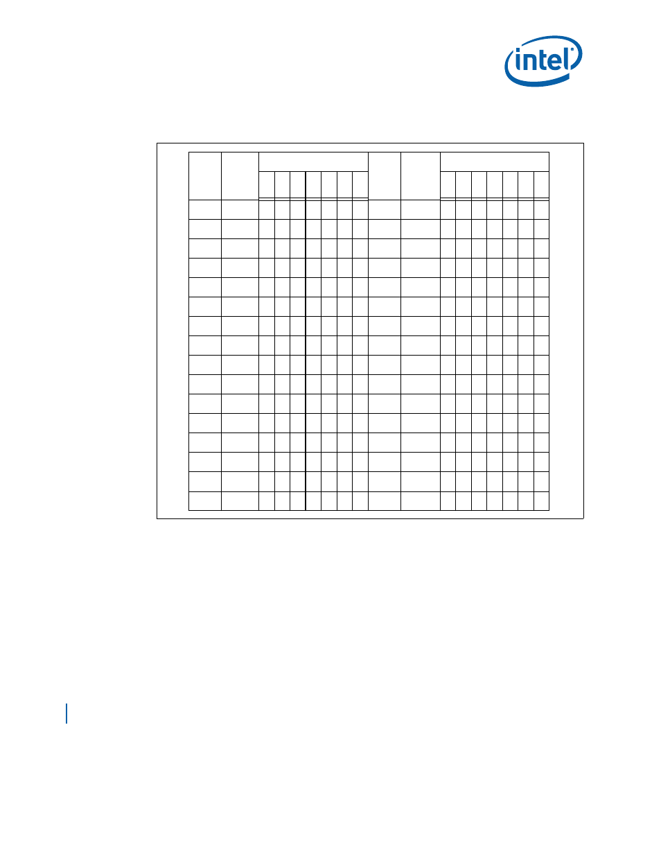
2 ecc generation for partial writes, 58 intel, Figure 58. intel – Intel CONTROLLERS 413808 User Manual
Page 521: Intel

Intel
®
413808 and 413812 I/O Controllers in TPER Mode
October 2007
Developer’s Manual
Order Number: 317805-001US
521
SRAM Memory Controller—Intel
®
413808 and 413812
8.3.3.2
ECC Generation for Partial Writes
If the memory transaction writes less than 32-bit data, then the SRAM Control Block
translates the write transaction into a read-modify-write transaction. For a partial write,
the SRAM Control Block calculates the ECC for the modified datum and writes it back.
So, if an external unit issues a write cycle with partial data to an SMCU port, the SMCU:
1. Issues a 32-bit read.
2. Modifies the value with the new portion to be written.
3. Calculates the ECC on the modified value.
4. Writes the 32-bit value and ECC.
Note:
If the SMCU detects a single-bit error during the read, it is corrected BEFORE being
merged with the write data so the corrected data is written back to the array. If a
multi-bit error is detected, the SMCU causes an interrupt to the core by writing to the
MCISR. The memory location is overwritten by the SMCU with the error data but valid
ECC, making the contents of memory invalid. For more details on how the SMCU
handles error conditions, see
Section 8.4, “ECC Interrupts/Error Conditions” on
Figure 58. Intel
®
413808 and 413812 I/O Controllers G-Matrix (generates the ECC)
Data
Bit
ECC
Code
ECC Check Bits (E[6:0]
Data
Bit
ECC
Code
ECC Check Bits (E[6:0]
E
6
E
5
E
4
E
3
E
2
E
1
E
0
E
6
E
5
E
4
E
3
E
2
E
1
E
0
D31
2CH
X
X
X
D15
45H
X
X
X
D30
4AH
X
X
X
D14
51H
X
X
X
D29
1AH
X
X
X
D13
43H
X
X
X
D28
29H
X
X
X
D12
61H
X
X
X
D27
5EH
X
X
X
X
X
D11
25H
X
X
X
D26
6BH
X
X
X
X
X
D10
31H
X
X
X
D25
2AH
X
X
X
D9
13H
X
X
X
D24
3BH
X
X
X
X
X
D8
5BH
X
X
X
X
X
D23
64H
X
X
X
D7
46H
X
X
X
D22
26H
X
X
X
D6
32H
X
X
X
D21
3EH
X
X
X
X
X
D5
23H
X
X
X
D20
15H
X
X
X
D4
68H
X
X
X
D19
34H
X
X
X
D3
4CH
X
X
X
D18
54H
X
X
X
D2
52H
X
X
X
D17
37H
X
X
X
X
X
D1
62H
X
X
X
D16
6EH
X
X
X
X
X
D0
49H
X
X
X
