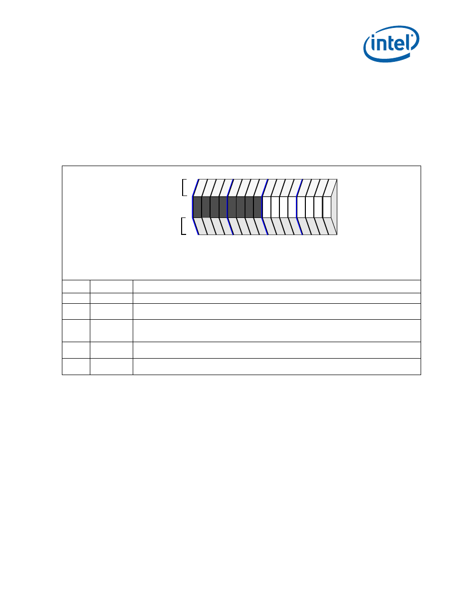
22 message control register - message_control, 287 message control register - message_control, Messaging unit—intel – Intel CONTROLLERS 413808 User Manual
Page 431: Bit default description, P_inta

Intel
®
413808 and 413812 I/O Controllers in TPER Mode
October 2007
Developer’s Manual
Order Number: 317805-001US
431
Messaging Unit—Intel
®
413808 and 413812
4.7.22
Message Control Register - Message_Control
The Message Control Register provides system software control over MSI. After reset,
MSI is disabled. System software is permitted to modify the Message Control register’s
read/write bits and fields while a device driver is not permitted to modify them.
Note:
Refer to the Peripheral Registers Chapter for the default internal bus address. This
register is part of the configuration space of the Address Translation Unit that is setup
as an endpoint.
Table 287. Message Control Register - Message_Control
Bit
Default
Description
15:8
00H
Reserved
7
1
2
64-bit Address Support - This field is set to 1
2
indicating that the 4138xx
is capable of generating a
64-bit message address.
6:4
000
2
Multiple Message Enable - System software writes to this field to indicate the number of messages
allocated to the 4138xx. While, the 4138xx
requests two messages, it is possible that system software
only allocates one message. The device hardware is designed to handle both cases.
3:1
001
2
Multiple Message Capable - This field is set to 001
2
indicating that the 4138xx
can issue up to two
unique interrupt messages.
0
0
2
MSI Enable - Setting this bit enables the 4138xx MSI functionality and disables the use of the
P_INTA#
interrupt output for 4138xx
interrupts
.
PCI
IOP
Attributes
Attributes
15
12
8
4
0
rv
rv
rv
rv
rv
rv
rv
rv
rv
rv
rv
rv
rv
rv
rv
rv
ro
ro
rw
rw
rw
rw
rw
rw
ro
ro
ro
ro
ro
ro
rw
rw
Attribute Legend:
RV = Reserved
PR = Preserved
RS = Read/Set
RW = Read/Write
RC = Read Clear
RO = Read Only
NA = Not Accessible
PCI Configuration Offset
A2H
Internal Bus Address Offset
0A2H
