38 expansion rom translate value register - ertvr, 38expansion rom translate value register - ertvr, 178 expansion rom translate value register - ertvr – Intel CONTROLLERS 413808 User Manual
Page 325: Address translation unit (pci express)—intel, Bit default description, Intel

Intel
®
413808 and 413812 I/O Controllers in TPER Mode
October 2007
Developer’s Manual
Order Number: 317805-001US
325
Address Translation Unit (PCI Express)—Intel
®
413808 and 413812
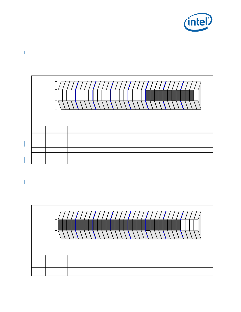
3.17.38 Expansion ROM Translate Value Register - ERTVR
The Expansion ROM Translate Value Register 0 (ERTVR) in conjunction with the
“Expansion ROM Upper Translate Value Register - ERUTVR” on page 325
contain bits 35
to 12 of the internal bus address used to convert PCI Express Link addresses. The
converted address is driven on the internal bus as a result of the Expansion ROM
address translation.
3.17.39 Expansion ROM Upper Translate Value Register - ERUTVR
The Expansion ROM Upper Translate Value Register (ERUTVR) in conjunction with the
“Expansion ROM Translate Value Register - ERTVR” on page 325
contain bits 35 to12 of
the internal bus address used to convert PCI Express Link addresses. The converted
address is driven on the internal bus as a result of the Expansion ROM address
translation.
Table 178. Expansion ROM Translate Value Register - ERTVR
Bit
Default
Description
31:12
00000H
Expansion ROM Translation Value - This value represents bits 31 to 12 of the internal bus address used
to convert the PCI address to internal bus addresses. This value must be naturally aligned with the
ERBAR register’s programmed value (see
Section 3.17.15, “Determining Block Sizes for Base
Address Registers” on page 306
).
11:01
000H
Reserved
00
0
Big Endian Byte Swap enable - When set the ATU performs a byte swap on all PCI read transactions
through ERBAR. When clear, no swap is performed. Refer to
Section 3.4, “Big Endian Byte Swapping” on
PCI
IOP
Attributes
Attributes
28
24
20
16
12
8
4
0
31
rw
rw
rw
rw
rw
rw
rw
rw
rw
rw
rw
rw
rw
rw
rw
rw
rw
rw
rw
rw
rw
rw
rw
rw
rw
rw
rw
rw
rw
rw
rw
rw
rw
rw
rw
rw
rw
rw
rw
rw
rv
rv
rv
rv
rv
rv
rv
rv
rv
rv
rv
rv
rv
rv
rv
rv
rv
rv
rv
rv
rv
rv
rw
rw
Attribute Legend:
RV = Reserved
PR = Preserved
RS = Read/Set
RW = Read/Write
RC = Read Clear
RO = Read Only
NA = Not Accessible
Internal Bus Address Offset
+068H
Table 179. Expansion ROM Upper Translate Value Register - ERUTVR
Bit
Default
Description
31:04
000 0000H Reserved
3:0
0H
Expansion ROM Upper Translation Value - This value represents bits 35 to 32 of the internal bus address
used to convert the PCI address to internal bus addresses.
PCI
IOP
Attributes
Attributes
28
24
20
16
12
8
4
0
31
rv
rv
rv
rv
rv
rv
rv
rv
rv
rv
rv
rv
rv
rv
rv
rv
rv
rv
rv
rv
rv
rv
rv
rv
rv
rv
rv
rv
rv
rv
rv
rv
rv
rv
rv
rv
rv
rv
rv
rv
rv
rv
rv
rv
rv
rv
rv
rv
rv
rv
rv
rv
rv
rv
rv
rv
rw
rw
rw
rw
rw
rw
rw
rw
Attribute Legend:
RV = Reserved
PR = Preserved
RS = Read/Set
RW = Read/Write
RC = Read Clear
RO = Read Only
NA = Not Accessible
Internal Bus Address Offset
+06CH
