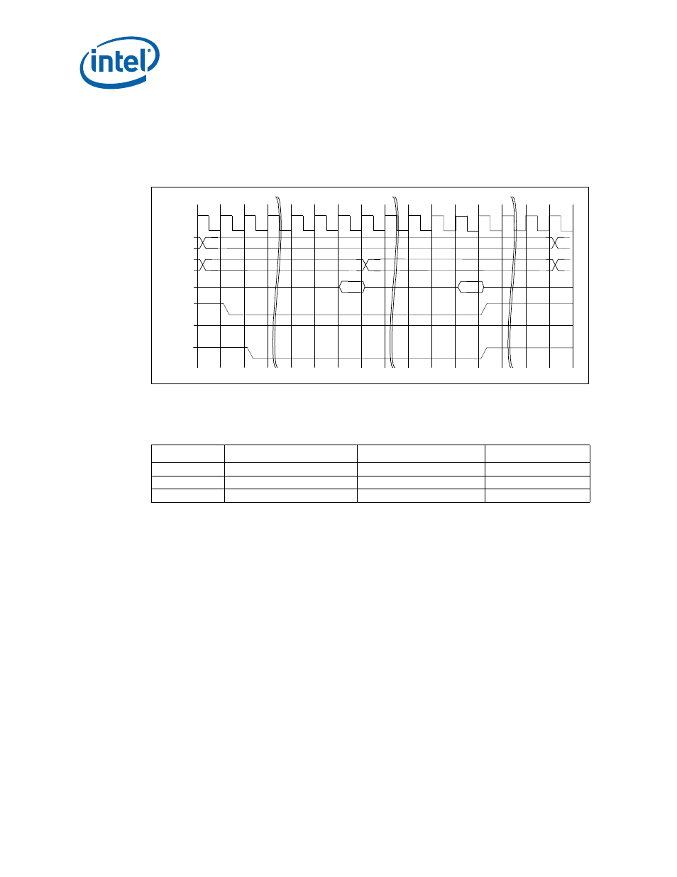
Figure 66. 120 ns flash burst read cycle, Table 362. flash wait state profile programming1, 66 120 ns flash burst read cycle – Intel CONTROLLERS 413808 User Manual
Page 552: 362 flash wait state profile programming, Table 362. flash wait state profile programming, Intel, Recovery wait states

Intel
®
413808 and 413812—Peripheral Bus Interface Unit
Intel
®
413808 and 413812 I/O Controllers in TPER Mode
Developer’s Manual
October 2007
552
Order Number: 317805-001US
illustrates a burst read cycle example for a 120 ns Flash device. This example
is illustrating a burst of two bytes or words. The PBI is capable of bursting up to four
bytes or words. The number of wait states used for address-to-data and data-to-data
are provided by the Address-to-Data Wait States and the Data-to-Data Wait States
field in PBBARx respectively.
Refer to
for the programmable address-to-data, data-to-data, and recovery
wait states. These numbers are based on a 66 MHz internal clock for the PBI interface.
Figure 66. 120 ns Flash Burst Read Cycle
A[24:03]
A[02:00]
Ta1
Tw1
Tw4
Td2
Tr1
Tr4
POE #
PWE #
PCEx #
Tw1
Tw8
Td2
D[15:00]
D_in
D_ in
Ti/Ta
Ta2
Td1
Td1
B6270-01
Table 362. Flash Wait State Profile Programming
Flash Speed Address-to-Data Wait States Data-to-Data Wait States
Recovery Wait States
<= 55 ns
4
4
1
<= 120 ns
8
4
4
<= 150 ns
12
4
4
Notes:
1.
Each Wait State represents a 15 ns period based on a 66 MHz clock. Refer to the appropriate Flash
device datasheets for programming accurate wait state numbers.
2.
Data-to-Data wait states are used for burst reads.
