Msi-x, Intel, Bit default description – Intel CONTROLLERS 413808 User Manual
Page 438: Msi-x table offset, Equation, Msi-x table bar indication register (bir)

Intel
®
413808 and 413812—Messaging Unit
Intel
®
413808 and 413812 I/O Controllers in TPER Mode
Developer’s Manual
October 2007
438
Order Number: 317805-001US
4.7.29
MSI-X Table Offset Register — MSI-X_Table_Offset
This register indicates in which PCI Memory Window the MSI-X Table is mapped. This
register also provides an offset in the specified PCI Memory Window of where the MSI-X
Table begins.
Note:
Refer to the Peripheral Registers Chapter for the default internal bus address. This
register is part of the configuration space of the Address Translation Unit that is setup
as an endpoint.
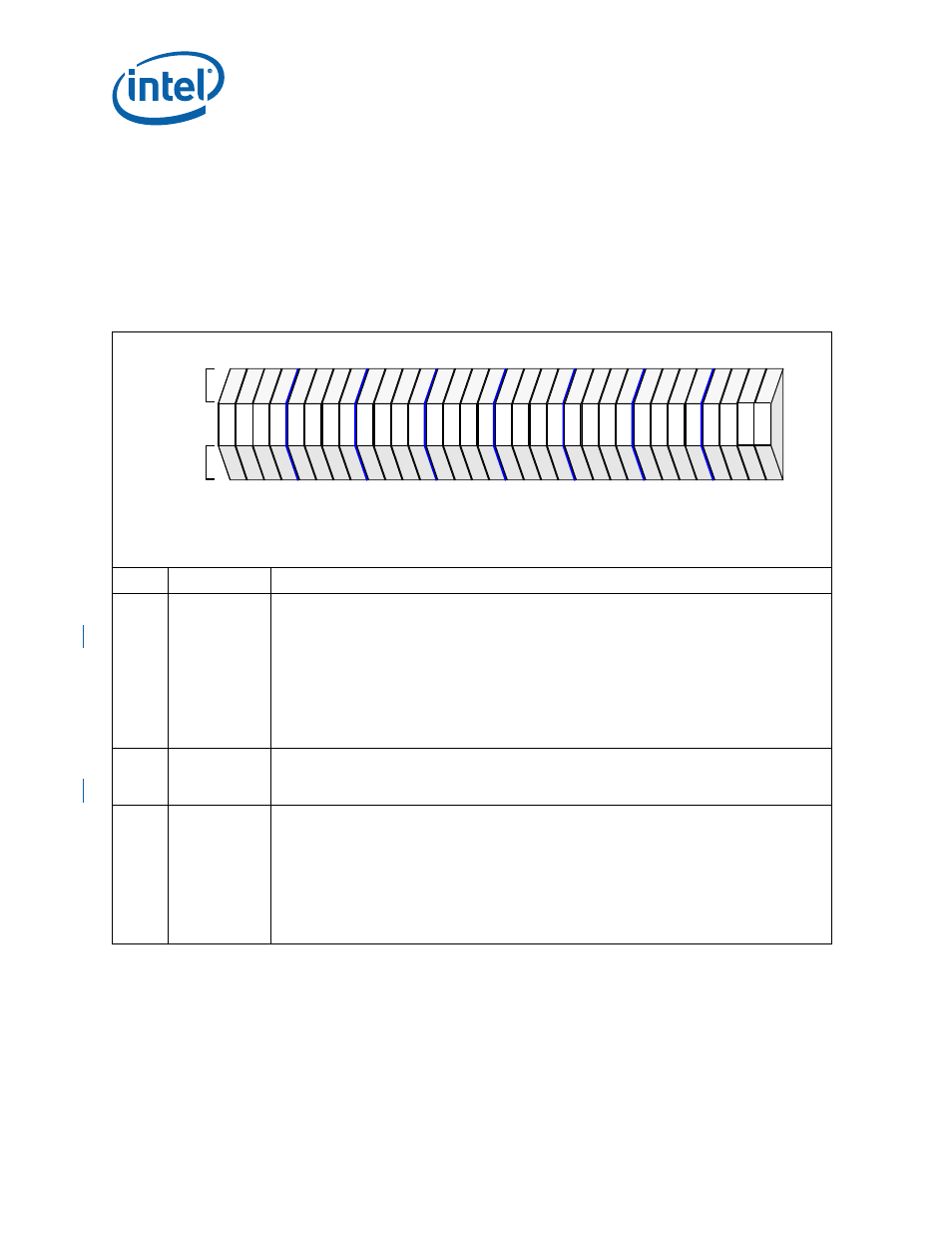
Table 294. MSI-X Table Offset Register - MSI-X_Table_Offset
Bit
Default
Description
31:13
0
MSI-X Table Offset:
Indicates the starting address of the MSI-X Table relative to the address in the
Base Address Register indicated bits [2:0] of this register. This part of the MSI-X Table Offset field is
programmable and is based on the value programmed in the
“MU Base Address Register - MUBAR” on
and the ATU Limit Value Register. The following equation may be used to compute MSI-X
Table Offset[31:13]. Note that the Messaging Unit occupies 8-KByte of address space and must
overlap the address space defined by the ATU Value and the ATU Limit registers.
Equation:
MSI-X Table Offset[31:13] = {(~ATU Limit_Register[31:0] & MU_Bar[31:0]} >> 13
Note:
The default location of the MU space after reset is in the first 8-KByte of the default ATU
Translation Window.
12:3 1_0000_0000_0
2
MSI-X Table Offset:
Indicates the starting address of the MSI-X Table relative to the address in the
Base Address Register indicated bits [2:0] of this register. This part of the MSI-X Table Offset field is
fixed which forces the table to offset at a 4-KByte offset relative to the
.
2:0
000
2
MSI-X Table BAR Indication Register (BIR)
: indicates which Base Address Register of the ATU
function the MSI-X Table is mapped into.
BIR Value Base Address Register
0 10H
1 14H
2 18H
3 1CH
4 20H
5 24H
All other values are reserved.
PCI
IOP
Attributes
Attributes
28
24
20
16
12
8
4
0
31
rw
ro
rw
ro
rw
ro
rw
ro
rw
ro
rw
ro
rw
ro
rw
ro
rw
ro
rw
ro
rw
ro
rw
ro
rw
ro
rw
ro
rw
ro
rw
ro
rw
ro
rw
ro
rw
ro
rv
ro
rv
ro
rv
ro
rv
ro
rv
ro
rv
ro
rv
ro
rv
ro
rv
ro
rv
ro
rw
ro
rw
ro
rw
ro
Attribute Legend:
RV = Reserved
PR = Preserved
RS = Read/Set
RW = Read/Write
RC = Read Clear
RO = Read Only
NA = Not Accessible
PCI Configuration Offset
B4 - B7H
Internal Bus Address Offset
0B4H
