Outbound configuration cycle data, Register - occdr, Intel – Intel CONTROLLERS 413808 User Manual
Page 382: Bit default description

Intel
®
413808 and 413812—Address Translation Unit (PCI Express)
Intel
®
413808 and 413812 I/O Controllers in TPER Mode
Developer’s Manual
October 2007
382
Order Number: 317805-001US
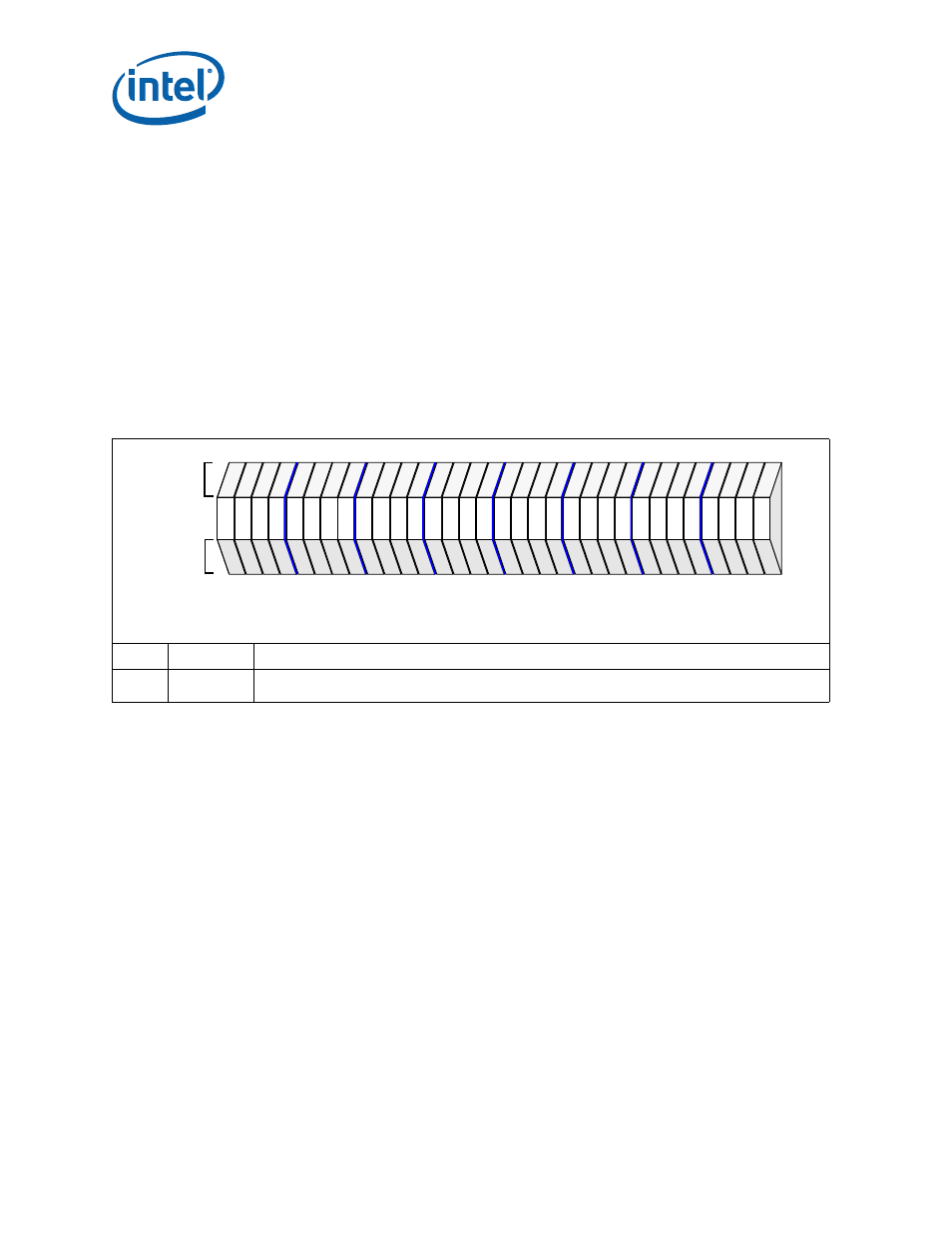
3.17.103 Outbound Configuration Cycle Data Register - OCCDR
The Outbound Configuration Cycle Data Register is used to initiate a configuration read
or write transaction on the PCI Express Link. The register is logical rather than physical
meaning that it is an address not a register. The Intel XScale
®
processor reads or
writes the data registers memory-mapped address to initiate the configuration
transaction on the PCI Express Link with the address found in the OCCAR. For a
configuration write, the data is latched from the internal bus and forwarded directly to
the ONPQ. For a read, the data is returned directly from the ICPLDQ to the Intel
XScale
®
processor and is never actually entered into the data register (which does not
physically exist).
The OCCDR is only visible from 4138xx internal bus address space and appears as a
reserved value within the ATU configuration space.
Note:
This register does not physically exist and reads from the PCI domain returns ‘0’.
Table 243. Outbound Configuration Cycle Data Register - OCCDR
Bit
Default
Description
31:00 0000 0000H Configuration Cycle Data - These bits define the data used during an outbound configuration read or
write transaction.
PCI
IOP
Attributes
Attributes
28
24
20
16
12
8
4
0
31
rw
ro
rw
ro
rw
ro
rw
ro
rw
ro
rw
ro
rw
ro
rw
ro
rw
ro
rw
ro
rw
ro
rw
ro
rw
ro
rw
ro
rw
ro
rw
ro
rw
ro
rw
ro
rw
ro
rw
ro
rw
ro
rw
ro
rw
ro
rw
ro
rw
ro
rw
ro
rw
ro
rw
ro
rw
ro
rw
ro
rw
ro
rw
ro
Attribute Legend:
RV = Reserved
PR = Preserved
RS = Read/Set
RW = Read/Write
RC = Read Clear
RO = Read Only
NA = Not Accessible
Internal Bus Address Offset
+330H
