1 inbound message register - imrx, Table 266. inbound message register - imrx, 2 outbound message register - omrx – Intel CONTROLLERS 413808 User Manual
Page 412: Table 267. outbound message register - omrx, 266 inbound message register - imrx, 267 outbound message register - omrx, Intel, Bit default description, Processor may be generated

Intel
®
413808 and 413812—Messaging Unit
Intel
®
413808 and 413812 I/O Controllers in TPER Mode
Developer’s Manual
October 2007
412
Order Number: 317805-001US
4.7.1
Inbound Message Register - IMRx
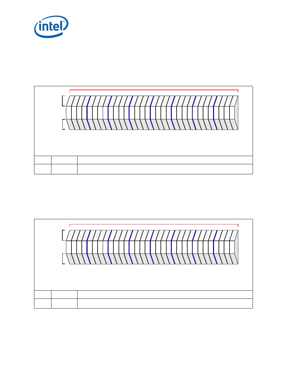
There are two Inbound Message Registers: IMR0 and IMR1. When the IMR register is
written, an interrupt to the Intel XScale
®
processor may be generated. The interrupt is
recorded in the Inbound Interrupt Status Register and may be masked by the Inbound
Message Interrupt Mask bit in the Inbound Interrupt Mask Register.
4.7.2
Outbound Message Register - OMRx
There are two Outbound Message Registers: OMR0 and OMR1. When the OMR register
is written, a Host I/O Interface interrupt may be generated. The interrupt is recorded in
the Outbound Interrupt Status Register and may be masked by the Outbound Message
Interrupt Mask bit in the Outbound Interrupt Mask Register.
Table 266. Inbound Message Register - IMRx
Bit
Default
Description
31:00 0000 0000H Inbound Message - This is a 32-bit message written by an external Host I/O Interface agent. When
written, an interrupt to the Intel XScale
®
processor may be generated.
PCI
IOP
Attributes
Attributes
28
24
20
16
12
8
4
0
31
rw
rw
rw
rw
rw
rw
rw
rw
rw
rw
rw
rw
rw
rw
rw
rw
rw
rw
rw
rw
rw
rw
rw
rw
rw
rw
rw
rw
rw
rw
rw
rw
rw
rw
rw
rw
rw
rw
rw
rw
rw
rw
rw
rw
rw
rw
rw
rw
rw
rw
rw
rw
rw
rw
rw
rw
rw
rw
rw
rw
rw
rw
rw
rw
Attribute Legend:
RV = Reserved
PR = Preserved
RS = Read/Set
RW = Read/Write
RC = Read Clear
RO = Read Only
NA = Not Accessible
MU/PCI Base Address Offset
IMR0: 0010H
IMR1: 0014H
internal bus address offset
IMR0: 4010H
IMR1: 4014H
Table 267. Outbound Message Register - OMRx
Bit
Default
Description
31:00
00000000H Outbound Message - This is 32-bit message written by the Intel XScale
®
processor. When written, an
interrupt may be generated on the PCI Interrupt pin determined by the ATU Interrupt Pin Register.
PCI
IOP
Attributes
Attributes
28
24
20
16
12
8
4
0
31
rw
rw
rw
rw
rw
rw
rw
rw
rw
rw
rw
rw
rw
rw
rw
rw
rw
rw
rw
rw
rw
rw
rw
rw
rw
rw
rw
rw
rw
rw
rw
rw
rw
rw
rw
rw
rw
rw
rw
rw
rw
rw
rw
rw
rw
rw
rw
rw
rw
rw
rw
rw
rw
rw
rw
rw
rw
rw
rw
rw
rw
rw
rw
rw
Attribute Legend:
RV = Reserved
PR = Preserved
RS = Read/Set
RW = Read/Write
RC = Read Clear
RO = Read Only
NA = Not Accessible
MU/PCI Base Address Offset
OMR0: 0018H
OMR1: 001CH
internal bus address offset
OMR0: 4018H
OMR1: 401CH
