21 expansion rom base address register - erbar, 21expansion rom base address register - erbar, 47 expansion rom base address register -erbar – Intel CONTROLLERS 413808 User Manual
Page 162: Intel, Bit default description

Intel
®
413808 and 413812—Address Translation Unit (PCI-X)
Intel
®
413808 and 413812 I/O Controllers in TPER Mode
Developer’s Manual
October 2007
162
Order Number: 317805-001US
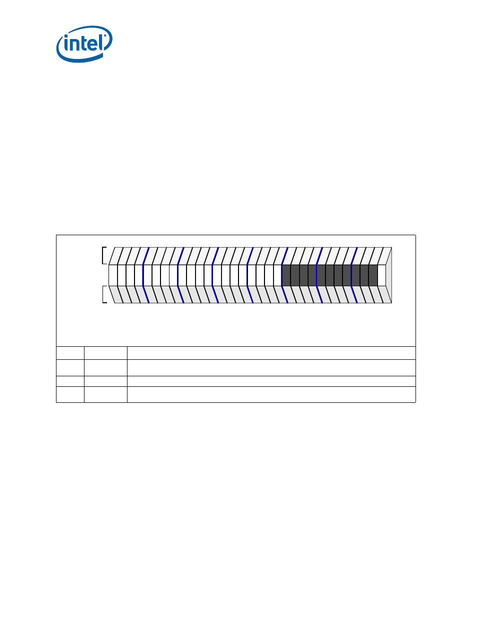
2.14.21 Expansion ROM Base Address Register - ERBAR
The Expansion ROM Base Address Register defines the block of memory addresses
used for containing the Expansion ROM. It permits the inclusion of multiple code
images, allowing the device to be initialized. The code image supplied consists of either
executable code or an interpreted code. Each code image must start on a 512 byte
boundary and each must contain the PCI Expansion ROM header. Image placement in
ROM space depends on the length of code images which precede it within ROM. ERBAR
defines the base address and describes the required memory block size; see
. Expansion ROM address space (limit size) can be a maximum of 16
MBytes. Bits 31 through 12 of the ERBAR is either read/write bits or read only with a
value of 0 depending on the value located within the ERLR. This configuration allows
the ERBAR to be programmed per PCI Local Bus Specification, Revision 2.3.
The Expansion ROM Base Address Register’s programmed value must comply with the
PCI programming requirements for address alignment. Refer to the PCI Local Bus
Specification, Revision 2.3 for additional information on programming Expansion ROM
base address registers.
Table 47. Expansion ROM Base Address Register -ERBAR
Bit
Default
Description
31:12
00000H
Expansion ROM Base Address - These bits define the actual location where the Expansion ROM address
window resides when addressed from the PCI bus on any 4 Kbyte boundary.
11:01
000H
Reserved
00
0
2
Address Decode Enable - This bit field shows the ROM address decoder is enabled or disabled. When
cleared, indicates the address decoder is disabled.
PCI
IOP
Attributes
Attributes
28
24
20
16
12
8
4
0
31
rw
rw
rw
rw
rw
rw
rw
rw
rw
rw
rw
rw
rw
rw
rw
rw
rw
rw
rw
rw
rw
rw
rw
rw
rw
rw
rw
rw
rw
rw
rw
rw
rw
rw
rw
rw
rw
rw
rw
rw
rv
rv
rv
rv
rv
rv
rv
rv
rv
rv
rv
rv
rv
rv
rv
rv
rv
rv
rv
rv
rv
rv
rw
rw
Attribute Legend:
RV = Reserved
PR = Preserved
RS = Read/Set
RW = Read/Write
RC = Read Clear
RO = Read Only
NA = Not Accessible
Register Offset
+030H
PCI Configuration Address Offset
30H - 33H
