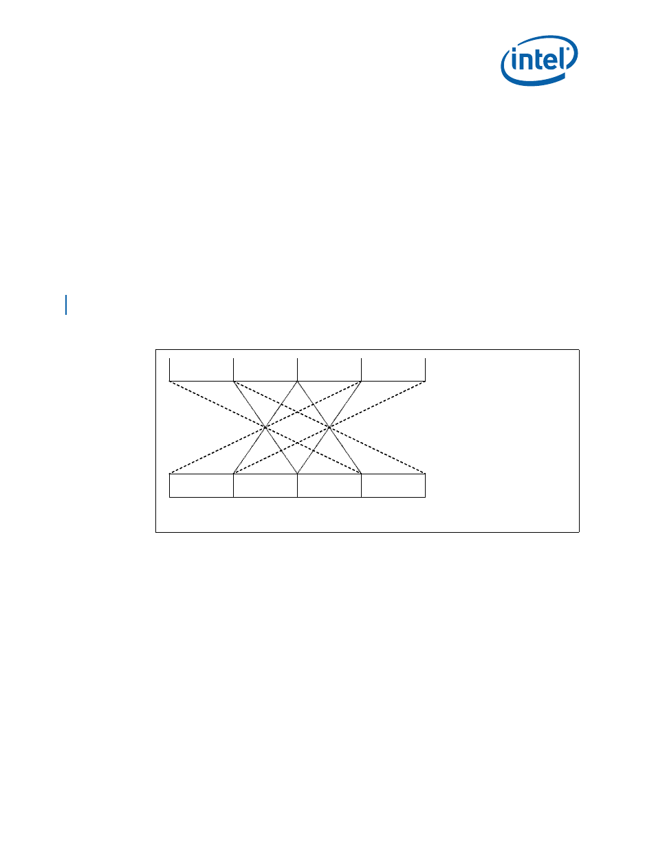
4 big endian byte swapping, 1 inbound byte swapping, Figure 28. inbound byte swapping – Intel CONTROLLERS 413808 User Manual
Page 255: 28 inbound byte swapping

Intel
®
413808 and 413812 I/O Controllers in TPER Mode
October 2007
Developer’s Manual
Order Number: 317805-001US
255
Address Translation Unit (PCI Express)—Intel
®
413808 and 413812
3.4
Big Endian Byte Swapping
Each memory and I/O window has an associated byte swapping enable located in the
following address translation registers:
• bit 0 of Inbound Address Translate Value Register 0-2 (IATVR0-2)
• bit 0 of Inbound Expansion ROM Translate Value Register (ERTVR)
• bit 0 of Outbound I/O Window Translate Value Register (OIOWTVR)
• bit 27 of Outbound Upper Memory BAR 0-3 (OUMBAR0-3)
Note:
The Messaging Unit (MU) Memory is mapped in PCI Window 0 (ATU Base Address
Register 0) along with the MSI-X table structures. Byte swapping should not be enabled
for BAR0 when using MSI-X.
3.4.1
Inbound Byte Swapping
When enabled, the swapping occurs as described in
. The bytes are swapped within a DWORD and byte swapping is
performed for all transactions regardless of byte count.
Figure 28. Inbound Byte Swapping
Byte 0 Byte 0
Word 0 [31:24] Word 0 [23:16]
Word 0 [15:8]
Word 0 [7:0]
Word 0 [7:0]
Word 0 [15:8]
Word 0 [23:16] Word 0 [31:24]
32-Bit Word on Internal Data Bus
32-Bit Word on PCI Bus
+3
+2
+1
+0
B6198-01
