9 atu cacheline size register - atuclsr, Table 35. atu cacheline size register - atuclsr, 10 atu latency timer register - atult – Intel CONTROLLERS 413808 User Manual
Page 152: Table 36. atu latency timer register - atult, 10atu latency timer register - atult, 35 atu cacheline size register - atuclsr, 36 atu latency timer register - atult, Atu cacheline size register - atuclsr, Atu cacheline size register, Atuclsr
Intel
®
413808 and 413812—Address Translation Unit (PCI-X)
Intel
®
413808 and 413812 I/O Controllers in TPER Mode
Developer’s Manual
October 2007
152
Order Number: 317805-001US
2.14.9
ATU Cacheline Size Register - ATUCLSR
Cacheline Size Register bit definitions adhere to PCI Local Bus Specification,
Revision 2.3. This register is programmed with the system cacheline size in DWORDs
(32-bit words). Cacheline Size is restricted to either 0, 8 or 16 DWORDs; the ATU
interprets any other value as “0”.
2.14.10 ATU Latency Timer Register - ATULT
ATU Latency Timer Register bit definitions apply to the PCI interface.
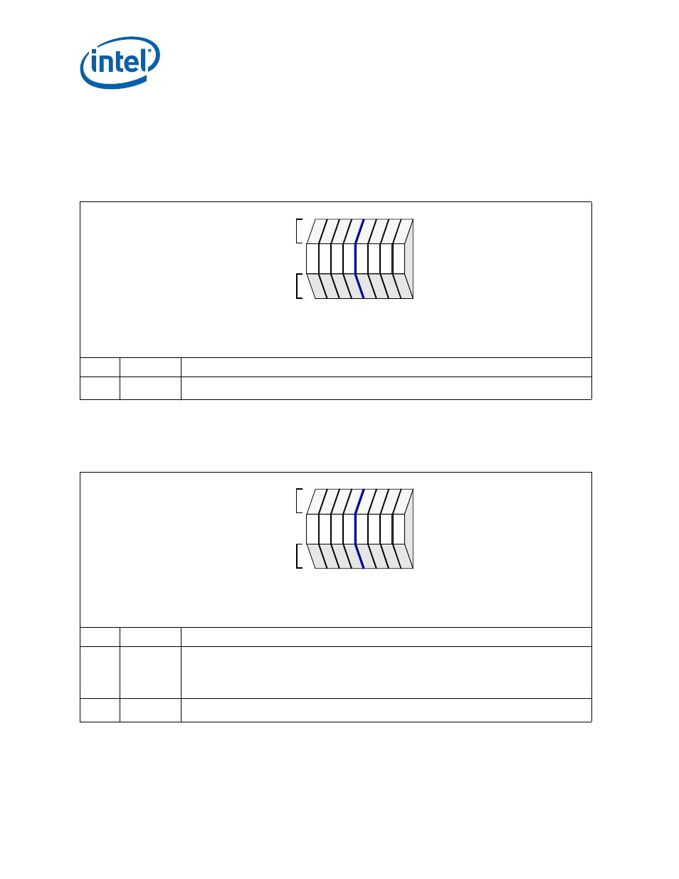
Table 35. ATU Cacheline Size Register - ATUCLSR
Bit
Default
Description
07:00
00H
ATU Cacheline Size - specifies the system cacheline size in DWORDs. Cacheline size is restricted to
either 0, 8 or 16 DWORDs.
PCI
IOP
Attributes
Attributes
7
4
0
rw
rw
rw
rw
rw
rw
rw
rw
rw
rw
rw
rw
rw
rw
rw
rw
Attribute Legend:
RV = Reserved
PR = Preserved
RS = Read/Set
RW = Read/Write
RC = Read Clear
RO = Read Only
NA = Not Accessible
Register Offset
+00CH
Table 36. ATU Latency Timer Register - ATULT
Bit
Default
Description
07:03
00000
2
(for
Conventional
mode)
01000
2
(for
PCI-X mode)
Programmable Latency Timer - This field varies the latency timer for the interface from 0 to 248 clocks.
The default value is 0 clocks for Conventional PCI mode, and 64 clocks for PCI-X mode.
02:00
000
2
Latency Timer Granularity - These Bits are read only giving a programmable granularity of 8 clocks for
the latency timer.
PCI
IOP
Attributes
Attributes
7
4
0
rw
rw
rw
rw
rw
rw
rw
rw
rw
rw
ro
ro
ro
ro
ro
ro
Attribute Legend:
RV = Reserved
PR = Preserved
RS = Read/Set
RW = Read/Write
RC = Read Clear
RO = Read Only
NA = Not Accessible
Register Offset
+00DH