48 vpd address register - vpdar, Table 188. vpd address register - vpdar, 49 vpd data register - vpddr – Intel CONTROLLERS 413808 User Manual
Page 336: Table 189. vpd data register - vpddr, 48vpd address register - vpdar, 49vpd data register - vpddr, 188 vpd address register - vpdar, 189 vpd data register - vpddr, Vpd address register, Intel
Intel
®
413808 and 413812—Address Translation Unit (PCI Express)
Intel
®
413808 and 413812 I/O Controllers in TPER Mode
Developer’s Manual
October 2007
336
Order Number: 317805-001US
3.17.48 VPD Address Register - VPDAR
The VPD Address register (VPDAR) contains the DWORD-aligned byte address of the
VPD to be accessed. The register is read/write and the initial value at power-up is
indeterminate.
A PCI Configuration Write to the VPDAR interrupts the Intel XScale
®
processor.
Software can use the Flag setting to determine whether the configuration write was
intended to initiate a read or write of the VPD through the VPD Data Register.
3.17.49 VPD Data Register - VPDDR
This register is used to transfer data between the 4138xx and the VPD storage
component.
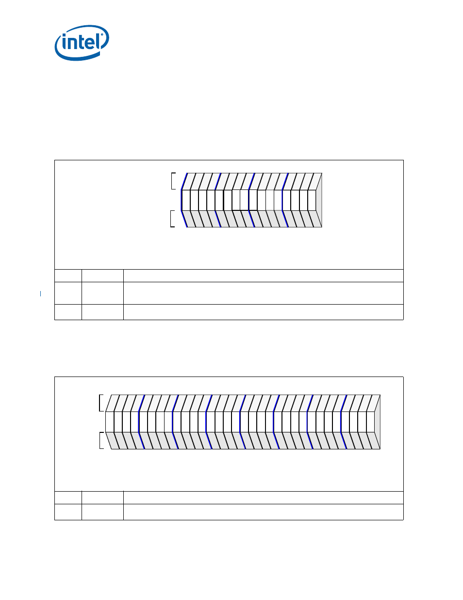
Table 188. VPD Address Register - VPDAR
Bit
Default
Description
15
0
2
Flag - A flag is used to indicate when a transfer of data between the VPD Data Register and the storage
component has completed. Please see
Section 3.13, “Vital Product Data” on page 282
for more details
on how the 4138xx
handles the data transfer.
14:0
0000H
VPD Address - This register is written to set the DWORD-aligned byte address used to read or write Vital
Product Data from the VPD storage component.
PCI
IOP
Attributes
Attributes
15
12
8
4
0
rw
rw
ro
rw
ro
rw
ro
rw
ro
rw
ro
rw
ro
rw
ro
rw
ro
rw
ro
rw
ro
rw
ro
rw
ro
rw
ro
rw
ro
rw
ro
rw
Attribute Legend:
RV = Reserved
PR = Preserved
RS = Read/Set
RW = Read/Write
RC = Read Clear
RO = Read Only
NA = Not Accessible
Internal Bus Address Offset
+092
Table 189. VPD Data Register - VPDDR
Bit
Default
Description
31:0
0000H
VPD Data - Four bytes are always read or written through this register to/from the VPD storage
component.
PCI
IOP
Attributes
Attributes
28
24
20
16
12
8
4
0
31
rw
rw
rw
rw
rw
rw
rw
rw
rw
rw
rw
rw
rw
rw
rw
rw
rw
rw
rw
rw
rw
rw
rw
rw
rw
rw
rw
rw
rw
rw
rw
rw
rw
rw
rw
rw
rw
rw
rw
rw
rw
rw
rw
rw
rw
rw
rw
rw
rw
rw
rw
rw
rw
rw
rw
rw
rw
rw
rw
rw
rw
rw
rw
rw
Attribute Legend:
RV = Reserved
PR = Preserved
RS = Read/Set
RW = Read/Write
RC = Read Clear
RO = Read Only
NA = Not Accessible
Internal Bus Address Offset
+094H