3 sgpio start drive lower register x - sgsdlrx, 3 sgpio start drive lower register x — sgsdlrx, 323 sgpio start drive lower register x — sgsdlrx – Intel CONTROLLERS 413808 User Manual
Page 478: Intel, Bit default description, Input[0:7, Output 3, Output 2, Output 1

Intel
®
413808 and 413812—SGPIO Unit
Intel
®
413808 and 413812 I/O Controllers in TPER Mode
Developer’s Manual
October 2007
478
Order Number: 317805-001US
6.6.3
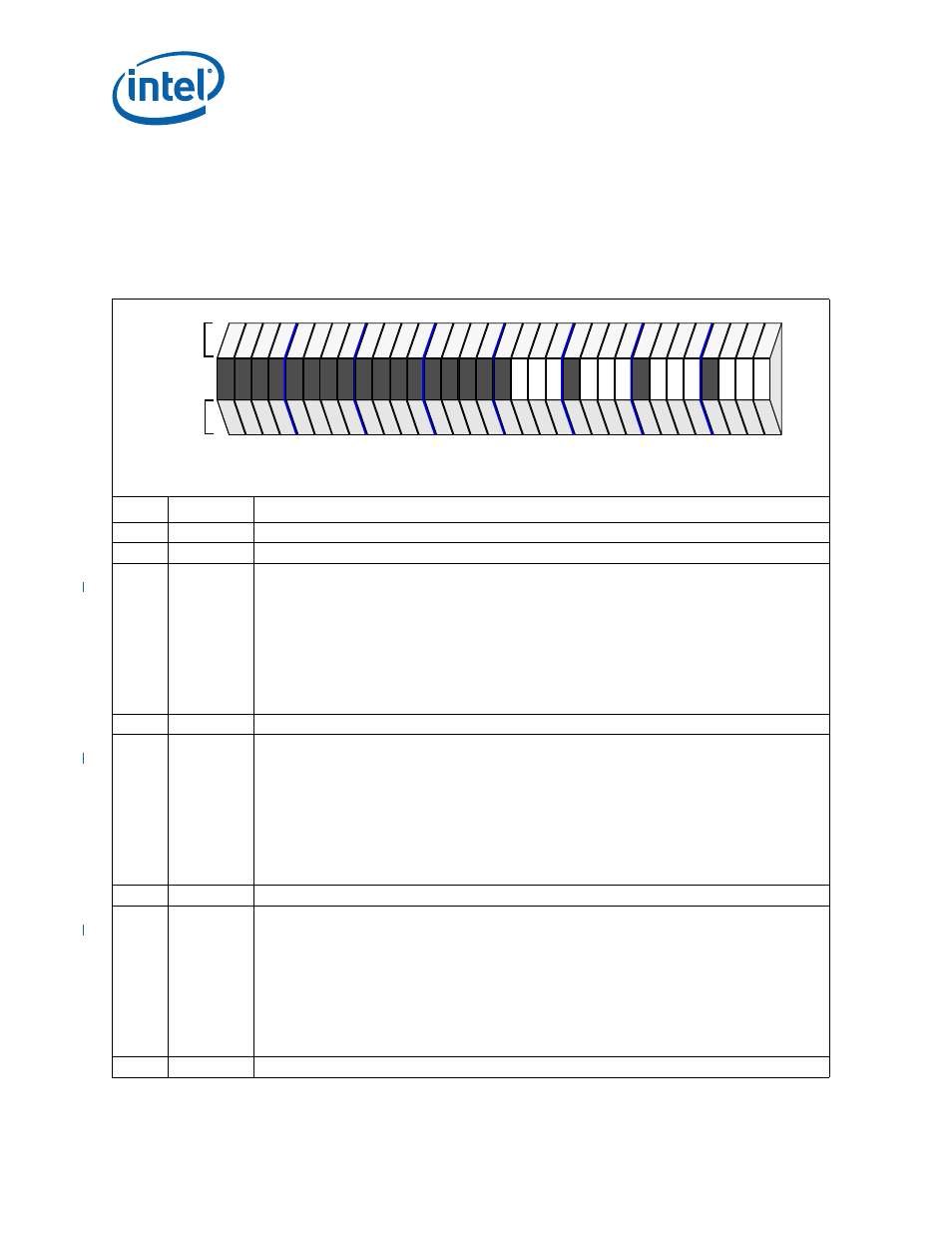
SGPIO Start Drive Lower Register x — SGSDLRx
The SGPIO Start Drive Lower Register x - SGSDLRx is used to program the drive
outputs order as they are shifted out on the serial bit stream. For example, after the
Vendor-Specific Code bits are shifted out on the SDataout pin, the user can choose in
which order each drive’s outputs are shifted out. This register controls the steering of
drive inputs[0:3] of the multiplexer block.
Table 323. SGPIO Start Drive Lower Register x — SGSDLRx (Sheet 1 of 2)
Bit
Default
Description
31:16
0000H
Reserved.
15
0
2
Reserved.
14:12
011
2
Output 3 Select Bits - This bit field selects which
Input[0:7]
of the Multiplexer Block is selected to drive
Output 3
. Refer to
Figure 52, “Output Signal Routing” on page 469
.
Bits Output Number
000
2
0
001
2
1
010
2
2
011
2
3
100
2
4
101
2
5
110
2
6
111
2
7
11
0
2
Reserved.
10:08
010
2
Output 2 Select Bits - This bit field selects which
Input[0:7]
of the Multiplexer Block is selected to drive
Output 2
. Refer to
Figure 52, “Output Signal Routing” on page 469
.
Bits Output Number
000
2
0
001
2
1
010
2
2
011
2
3
100
2
4
101
2
5
110
2
6
111
2
7
07
0
2
Reserved.
06:04
001
2
Output 1 Select Bits - This bit field selects which
Input[0:7]
of the Multiplexer Block is selected to drive
Output 1
. Refer to
Figure 52, “Output Signal Routing” on page 469
.
Bits Output Number
000
2
0
001
2
1
010
2
2
011
2
3
100
2
4
101
2
5
110
2
6
111
2
7
03
0
2
Reserved.
Coprocessor
IOP
Attributes
Attributes
28
24
20
16
12
8
4
0
31
rv
na
rv
na
rv
na
rv
na
rv
na
rv
na
rv
na
rv
na
rv
na
rv
na
rv
na
rv
na
rv
na
rv
na
rv
na
rv
na
rv
na
rw
na
rw
na
rw
na
rv
na
rw
na
rw
na
rw
na
rv
na
rw
na
rw
na
rw
na
rv
na
rw
na
rw
na
rw
na
SGPIO #
0
1
Intel XScale
®
processor internal bus address offset
+2608H
+2688H
Attribute Legend:
RV = Reserved
PR = Preserved
RS = Read/Set
RW = Read/Write
RC = Read Clear
RO = Read Only
NA = Not Accessible
