2 flash write cycle, Figure 67. 120 ns flash single write cycle1, 67 120 ns flash single write cycle – Intel CONTROLLERS 413808 User Manual
Page 553: Strb, strh

Intel
®
413808 and 413812 I/O Controllers in TPER Mode
October 2007
Developer’s Manual
Order Number: 317805-001US
553
Peripheral Bus Interface Unit—Intel
®
413808 and 413812
9.2.6.2
Flash Write Cycle
Address-to-data and recovery wait states for reads and writes are identical and
programmed in PBBAR0 and PBBAR1. Refer to
for the programmable
address-to data wait states. However, Any write transactions issued to a Peripheral
address space window must always represent a single peripheral bus data cycle (
strb,
strh
) depending on the bus width selected in PBBAR0 — PBBAR1.
The PBI supports multi-byte write requests from the internal bus agents. Multi-byte
read and write requests are supported differently by the PBI. Write requests are limited
to a maximum of four bytes only and must not span a DWORD boundary. For a write
request with an address and byte-count combination that spans a DWORD boundary,
the PBI signals an address error and set bit 0 of the
“PBI Status Register — PBISR” on
. Unlike multi-byte read requests, the PBI supports multi-byte write requests
by breaking the writes on the PBI bus into multiple single data write transactions. The
number of single data write transactions initiated on the PBI bus are dependent to the
PBI bus width. For example, an aligned DWORD write on an 8-bit PBI bus turns into
four single 8-bit write transactions on the PBI bus, and an aligned DWORD write
request on a 16-bit PBI bus turns into two single 16-bit write transactions on the PBI
bus.
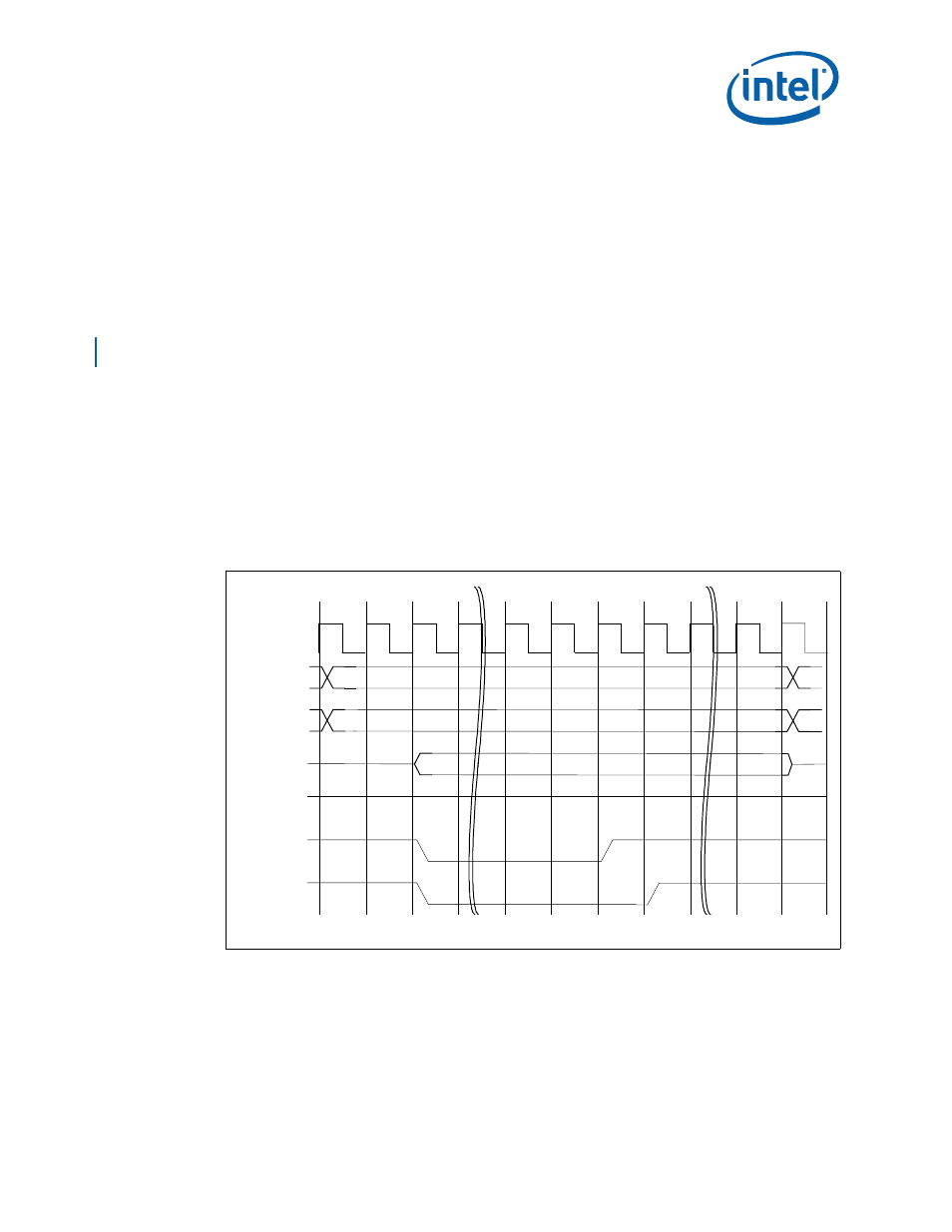
shows the only type of write transaction supported by the PBI bus. For
example, each write transaction ends after one data transfer to a single address
location regardless of bus width.
illustrates a write cycle example for a 120 ns Flash device. Both 8- and 16-bit
wide bus timings are identical.
Figure 67. 120 ns Flash Single Write Cycle
1
Notes:
1.
The PBI bus does not burst write transactions. A multi-byte write request made to the PBI is translated
into multiple single data write transactions on the PBI bus. And the number of single data write
transactions initiated on the PBI bus are dependent to the PBI bus width.
A[24:03]
A[02:00]
Ta2
Tw1
Tw8
Td2
Tr1
Tr4
POE #
PWE#
PCEx#
D[15:00]
D_out
Ti/Ta
Ta1
Td 1
B6271-01
