4 secondary clock outputs, Table 510. secondary clock output control, 510 secondary clock output control – Intel CONTROLLERS 413808 User Manual
Page 767: P_clko[3:0, P_clkout, Refclk
Intel
®
413808 and 413812 I/O Controllers in TPER Mode
October 2007
Developer’s Manual
Order Number: 317805-001US
767
Clocking and Reset—Intel
®
413808 and 413812
17.1.1.2.4 Secondary Clock Outputs
This component has the ability to provide four PCI bus clocks (
P_CLKO[3:0]
) to drive
external components as well as a dedicated feedback clock (
P_CLKOUT
) to drive the
ATUX PCI interface. These clock outputs are can only be used when the PCI Express
reference clock (
REFCLK+/-
) is used as the primary chip clock and the ATUX is
enabled and configured to operate as a Central Resource.
1
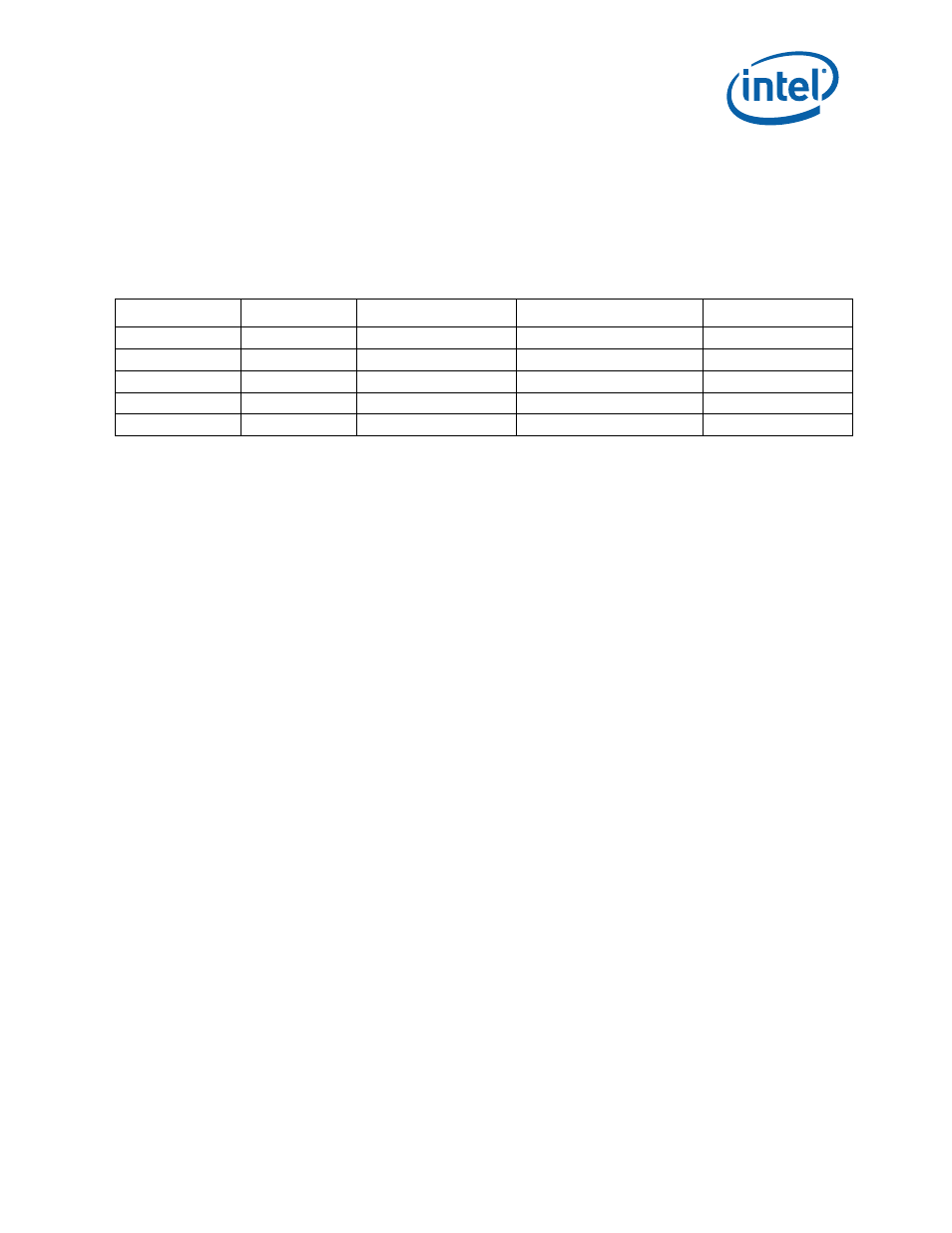
Table 510. Secondary Clock Output Control
PCIX_EP#
CLK_SRC_PCIE# INTERFACE_SEL_PCIX# PCIX/PCIe Interfaces Active Clock Outputs Enabled
0 (End Point)
–
–
–
No
1 (Central Resource)
1 (PCLKIN)
–
–
No
1 (Central Resource)
0 (REFCLK+/-)
1 (PCIe)
–
No
1 (Central Resource)
0 (REFCLK+/-)
0 (PCIX)
–
Yes
1 (Central Resource)
0 (REFCLK+/-)
–
Dual Interface
Yes