1 sram base address register - srambar, Table 350. sram base address register - srambar, 2 sram upper base address register - sramubar – Intel CONTROLLERS 413808 User Manual
Page 536: 3 sram ecc control register - secr, 1 sram base address register — srambar, 2 sram upper base address register — sramubar, 3 sram ecc control register — secr, 350 sram base address register — srambar, 351 sram upper base address register — sramubar, Table 350. sram base address register — srambar

Intel
®
413808 and 413812—SRAM Memory Controller
Intel
®
413808 and 413812 I/O Controllers in TPER Mode
Developer’s Manual
October 2007
536
Order Number: 317805-001US
8.6.1
SRAM Base Address Register — SRAMBAR
This register indicates the lower twelve bits of the beginning address (base address) of
SRAM memory array space. The SRAM is addressed using a 36-bit address. This
register is used in conjunction with the
Section 8.6.2, SRAM Upper Base Address
. After reset the default starting address of the SRAM memory is
0 FFE0 0000H.
Note:
SRAM memory space must
never
cross a 1 Mbyte boundary.
8.6.2
SRAM Upper Base Address Register — SRAMUBAR
This register indicates the upper four bits of the beginning address (base address) of
SRAM memory array space. The SRAM is addressed using a 36-bit address. This
register is used in conjunction with the
Section 8.6.1, SRAM Base Address Register —
. After reset the default starting address of the SRAM memory is 0 FFE0
0000H.
Note:
SRAM memory space must
never
cross a 1 Mbyte boundary.
8.6.3
SRAM ECC Control Register — SECR
This register programs the SMCU error correction and detection capabilities. The
configuration depends on the application’s needs but a typical configuration is:
• ECC Mode Enabled
• Enable multi-bit error reporting
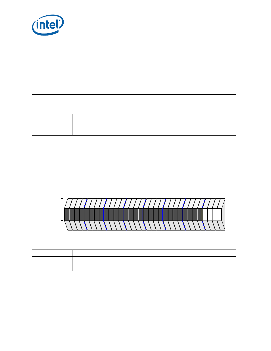
Table 350. SRAM Base Address Register — SRAMBAR
Bit
Default
Description
31:20
1111 1111
1110
2
SRAM Base Address:
Provide lower twelve bits of SRAM base address. Default SRAM base address is 0
FFE0 0000H.
19:00
0 0000H Reserved
Attribute Legend:
RV = Reserved
PR = Preserved
RS = Read/Set
RW = Read/Write
RC = Read Clear
RO = Read Only
NA = Not Accessible
Intel XScale
®
processor Local Bus Address
Offset
+ 1500H
Table 351. SRAM Upper Base Address Register — SRAMUBAR
Bit
Default
Description
31:04
0000 000H Reserved
03:00
0H
SDRAM Upper Base Address:
These bits define the upper four bits of the SRAM base address. The
default SRAM base address is 0 FFE0 0000H.
PCI
IOP
Attributes
Attributes
28
24
20
16
12
8
4
0
31
rv
na
rv
na
rv
na
rv
na
rv
na
rv
na
rv
na
rv
na
rv
na
rv
na
rv
na
rv
na
rv
na
rv
na
rv
na
rv
na
rv
na
rv
na
rv
na
rv
na
rv
na
rv
na
rv
na
rv
na
rv
na
rv
na
rv
na
rv
na
rw
na
rw
na
rw
na
rw
na
Attribute Legend:
RV = Reserved
PR = Preserved
RS = Read/Set
RW = Read/Write
RC = Read Clear
RO = Read Only
NA = Not Accessible
Intel XScale
®
processor Local Bus Address
Offset
+1504H
