Register descriptions pxdr – Cirrus Logic EP93xx User Manual
Page 800
28-10
DS785UM1
Copyright 2007 Cirrus Logic
GPIO Interface
EP93xx User’s Guide
2
8
2
8
28
1. A read from the data register returns the value of the GPIO module input port. These ports have a
default pin assignment. The read value default is the pin state based on the default pin map.
2. Port E bits 1 and 0 provide the LED driver function. The Port E[1:0] defaults to drive high. A read from
the Port E data register would be expected to return 0x03, if the other pins mapped to Port E inputs are
zero. However since the Port E[7:2] inputs are mapped to IDE control signals, the default read value will
depend on the default action of the IDE controller and the external interface.
3. The RAWSTATUSx registers have pin dependent default read states. The interrupt control registers
default to low level sensitive interrupt on reset. Therefore the external pin state will ripple through the
interrupt logic to determine the RAWSTATUSx default.
Register Descriptions
PxDR
Address:
0x8084_0050
GPIOFIntType2 R/W
GPIOFIntType2
0x00
0x8084_0054
Reserved, Read undefined
Write Only
GPIOFEOI
0x00
0x8084_0058 GPIOFIntEn
R/W
GPIOFIntEn
0x00
0x8084_005C IntStsF
Read
only
-
0x00
0x8084_0060 RawIntStsF
Read
only
-
Note
3
0x8084_0064 GPIOFDB
R/W
GPIOFDB
0x00
0x8084_0090 GPIOAIntType1
R/W
GPIOAIntType1
0x00
0x8084_0094 GPIOAIntType2
R/W
GPIOAIntType2
0x00
0x8084_0098 -
Write
Only
GPIOAEOI
-
0x8084_009C GPIOAIntEn
R/W
GPIOAIntEn
0x00
0x8084_00A0 IntStsA
Read
only
-
0x00
0x8084_00A4 RawIntStsA
Read
only
-
Note
3
0x8084_00A8 GPIOADB
R/W
GPIOADB
0x00
0x8084_00AC GPIOBIntType1
R/W
GPIOBIntType1
0x00
0x8084_00B0 GPIOBIntType2
R/W
GPIOBIntType2
0x00
0x8084_00B4 -
Write
Only
GPIOBEOI
-
0x8084_00B8 GPIOBIntEn
R/W
GPIOBIntEn
0x00
0x8084_00BC IntStsB
Read
only
-
0x00
0x8084_00C0 RawIntStsB
Read
only
-
Note
3
0x8084_00C4 GPIOBDB
R/W
GPIOBDB
0x00
0x8084_00C8 EEDrive
R/W
EEDrive
0x00
31
30
29
28
27
26
25
24
23
22
21
20
19
18
17
16
RSVD
15
14
13
12
11
10
9
8
7
6
5
4
3
2
1
0
RSVD
PxDATA
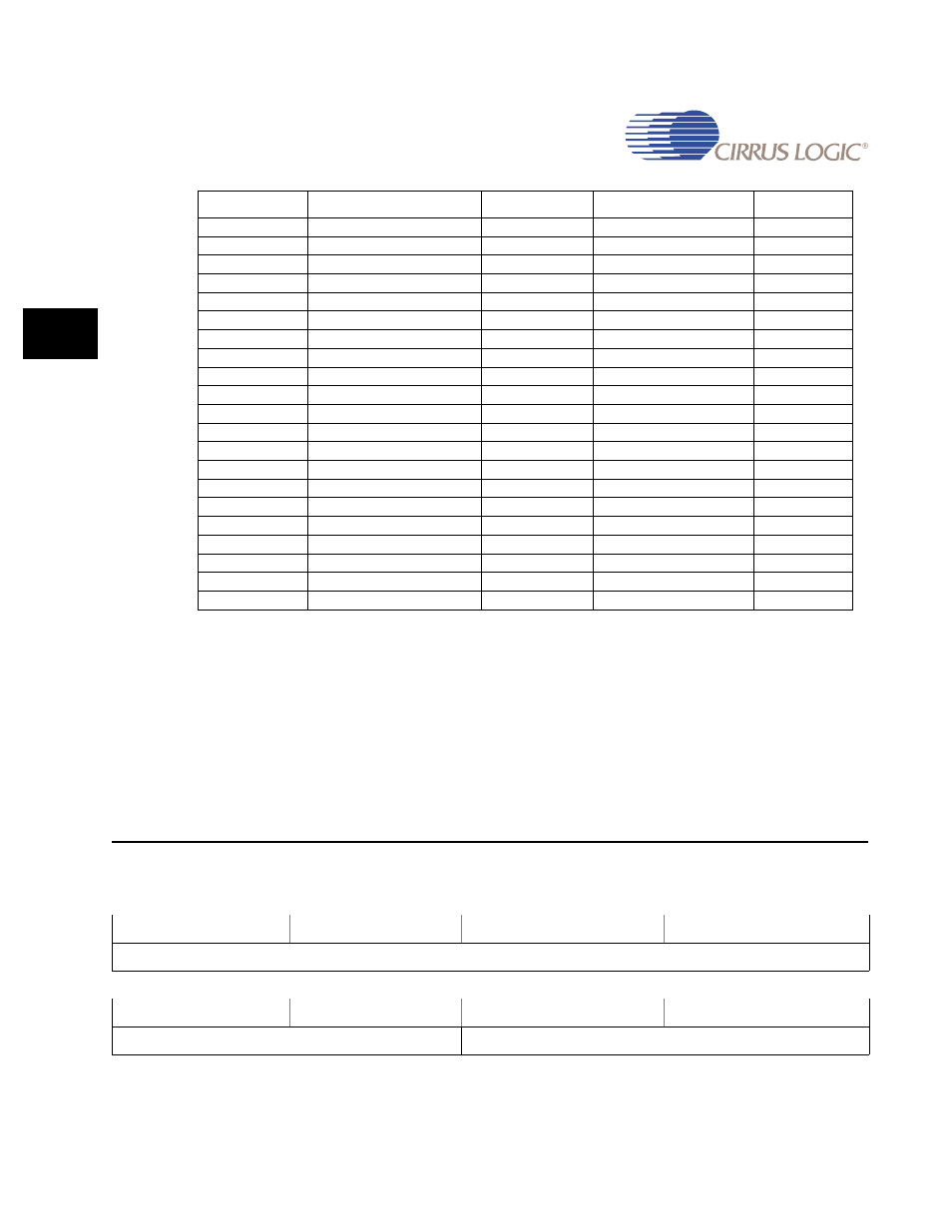
Table 28-5. GPIO Register Address Map (Continued)
Address
Read Location
Type
Write Location
Reset Value