Cirrus Logic EP93xx User Manual
Page 510
D
S
7
85U
M
1
13-1
4
C
o
pyr
ig
h
t 20
07
C
ir
ru
s
Lo
gic
S
D
RAM, Sy
nc
ROM, a
n
d
Sy
n
c
FLASH Co
ntrolle
r
EP93
xx U
ser
’s
G
u
ide
13
13
13
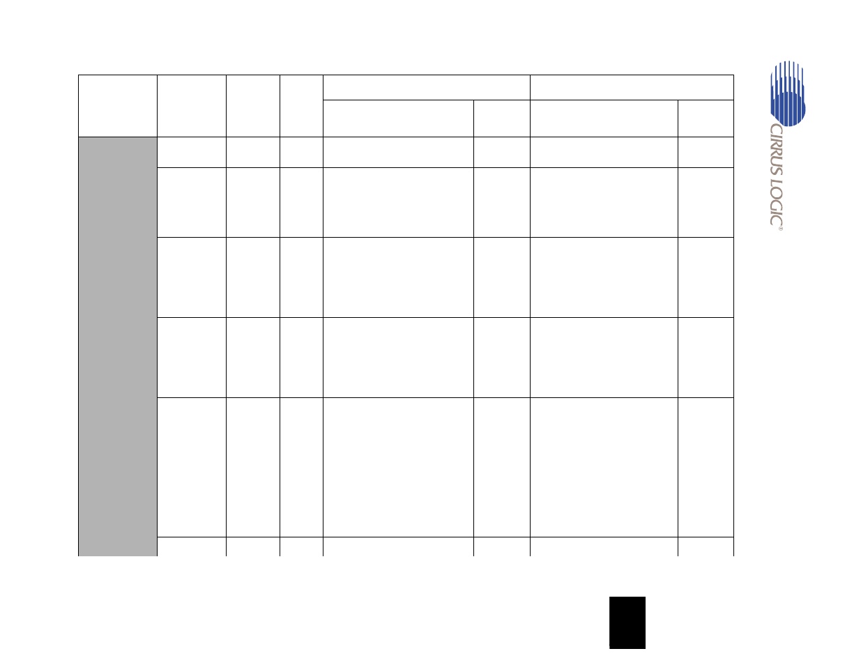
32-Bit Wide
Data Systems
64 Mbit (32-bit
wide device)
12 x 8 x 2
banks
8
Mbytes
0xN000_0000 - 0xN03F_FFFF
0xN400_0000 - 0xN43F_FFFF
4 Mbytes
0xN000_0000 - 0xN07F_FFFF
8 Mbytes
0xN000_0000 - 0xN01F_FFFF
0xN000_0000 - 0xN01F_FFFF
64 Mbit (32-bit
wide device)
11 x 8 x 4
banks
8
Mbytes
0xN400_0000 - 0xN41F_FFFF
0xN800_0000 - 0xN81F_FFFF
2 Mbytes
0xN040_0000 - 0xN05F_FFFF
0xN080_0000 - 0xN09F_FFFF
2 Mbytes
0xNC00_0000 - 0xNC1F_FFFF
0xN0C0_0000 - 0xN0DF_FFFF
0xN000_0000 - 0xN03F_FFFF
64 Mbit (2 x
16-bit wide
device)
12 x 8 x 4
banks
16
Mbytes
0xN400_0000 - 0xN43F_FFFF
0xN800_0000 - 0xN83F_FFFF
4 Mbytes
0xN000_0000 - 0xN0FF_FFFF
16 Mbytes
0xNC00_0000 - 0xNC3F_FFFF
0xN000_0000 - 0xN03F_FFFF
128 Mbit (32-
bit wide
device)
12 x 8 x 4
banks
16
Mbytes
0xN400_0000 - 0xN43F_FFFF
0xN800_0000 - 0xN83F_FFFF
4 Mbytes
0xN000_0000 - 0xN0FF_FFFF
16 Mbytes
0xNC00_0000 - 0xNC3F_FFFF
0xN000_0000 - 0xN03F_FFFF
0xN100_0000 - 0xN13F_FFFF
0xN400_0000 - 0xN43F_FFFF
128 Mbit (2 x
16-bit wide
device)
12 x 9 x 4
banks
32
Mbytes
0xN500_0000 - 0xN53F_FFFF
0xN800_0000 - 0xN83F_FFFF
0xN900_0000 - 0xN93F_FFFF
4 Mbytes
0xN000_0000 - 0xN1FF_FFFF
32 Mbytes
0xNC00_0000 - 0xNC3F_FFFF
0xND00_0000 - 0xND3F_FFFF
0xN000_0000 - 0xN07F_FFFF
Table 13-11. EP93xx SDRAM Address Ranges (16-Bit Wide Data Systems) (Continued)
Organization
Device
Size,
Type
System
Address
Matrix
Total
Bank
Size
SROMLL = 0
SROMLL = 1
Continuous Address
Range (see Note)
Size of
Segment
Continuous Address
Range (see Note)
Size of
Segment