2 internal m2p/p2m channel register map, 2 internal m2p/p2m channel register map -21 – Cirrus Logic EP93xx User Manual
Page 415

DS785UM1
10-21
Copyright 2007 Cirrus Logic
DMA Controller
EP93xx User’s Guide
1
0
1
0
10
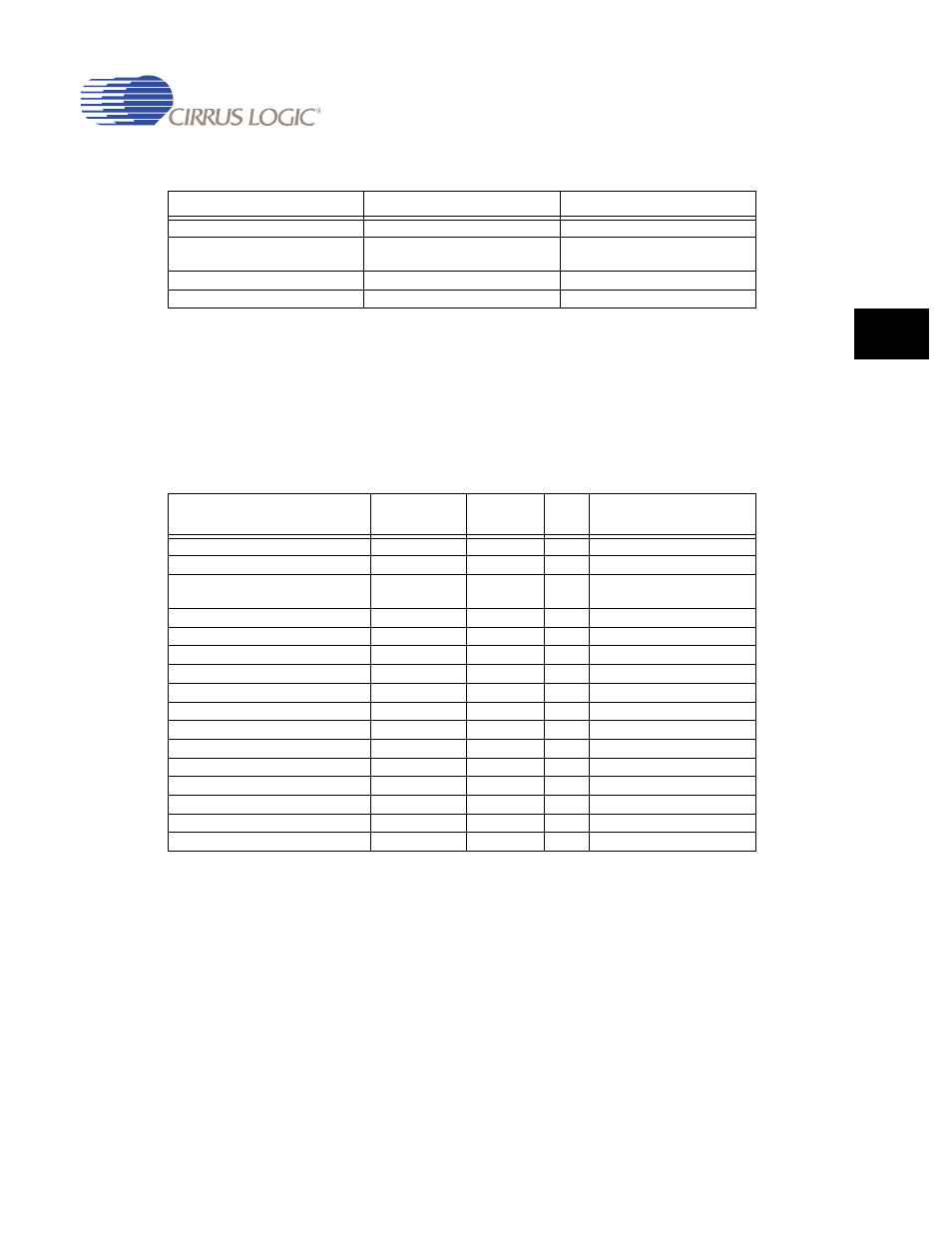
10.2.2 Internal M2P/P2M Channel Register Map
The DMA Memory Map above includes the base address mapping for the channel registers
for each of the 10 M2P/P2M channels that are shown in the following table, the Internal
M2P/P2M Channel Register Map. This mapping is common for each channel thus offset
addresses from the bases in
are shown in
for Channel Base Addresses
Note:* - write this location once to clear the interrupt (see Interrupt register description
for which bits this rule applies to).
0x8000_0340 -> 0x8000_037C
M2P Channel 8 Registers (Tx)
0x8000_0340
0x8000_0380
DMA Channel Arbitration
register
0x8000_03C0
DMA Global Interrupt register
0x8000_03C4 -> 0x8000_FFFC
Not Used
0x8000_03C4
Table 10-4. Internal M2P/P2M Channel Register Map
Offset
Register
Name
Access
Bits
Reset Value
Channel Base Address + 0x0000
R/W
6 0
Channel Base Address + 0x0004
R/W TC *
3
0
Channel Base Address + 0x0008
R/W
4
Channel dependant
(see register description)
Channel Base Address + 0x000C
RO
8
0
Channel Base Address + 0x0010
Reserved
Channel Base Address + 0x0014
RO
16
0
Channel Base Address + 0x0018
Reserved
Channel Base Address + 0x001C
Reserved
Channel Base Address + 0x0020
R/W
16
0
Channel Base Address + 0x0024
R/W
32
0
Channel Base Address + 0x0028
RO
32
0
Channel Base Address + 0x002C
Reserved
Channel Base Address + 0x0030
R/W
16
0
Channel Base Address + 0x0034
R/W
32
0
Channel Base Address + 0x0038
RO
32
0
Channel Base Address + 0x003C
Reserved
Table 10-3. DMA Memory Map
ARM920T Address
Description
Channel Base Address
